|
Design Techniques for EMC – Part 6 ESD, Dips, Flicker, Dropouts, Electromechanical Switching, and Power Factor Correction By
Eur Ing Keith Armstrong CEng MIEE MIEEE |
This is the final part of a series of six articles on best-practice EMC techniques in electrical/electronic/mechanical hardware design. The series is intended for the designer of electronic products, from building block units such as power supplies, single-board computers, and “industrial components” such as motor drives, through to stand-alone or networked products such as computers, audio/video/TV, instruments, etc.
The techniques covered in the six articles are:
1) Circuit design (digital, analogue, switch-mode, communications), and choosing components
2) Cables and connectors
3) Filters and transient suppressers
4) Shielding
5) PCB layout (including transmission lines)
6) ESD, dips, flicker, dropouts, electromechanical switching, and power factor correction
A textbook could be written about any one of the above topics (and many have), so this magazine article format can only introduce the various issues and point to the most important best-practice techniques. Many of the techniques described in this series are also important for improving signal integrity: reducing the number of iterations during development and reducing manufacturing costs.
Table of contents for this part
6. A number of specific issues
6.1 Electrostatic Discharge (ESD)
6.1.2 The "Human Body Model" and ESD testing
6.1.3 Design techniques for personnel ESD
6.1.6 Adding impedance to signal lines
6.1.7 Transient Voltage Suppressors (TVSs)
6.1.8 Low-pass filtering the signal lines
6.1.9 Common-mode filtering at connectors
6.1.10 Galvanic isolation techniques for ESD
6.1.11 Dealing with signal corruption
6.2 Dips, sags, brownouts, swells, dropouts, interruptions and power outages
6.3 Emissions of voltage fluctuations and flicker
6.4 The influence of the supply inductance
6.4.1 Reducing emissions from fluctuating DC loads
6.5 Electromechanical switching
6.5.1 Suppressing arcs and sparks at switches, relays, and contactors
6.5.2 Suppressing arcs and sparks in DC motors
6.5.3 Suppressing arcs and sparks in electric bells
6. A number of specific issues
The previous parts of this series focussed on design techniques which will benefit a large number of emissions and immunity characteristics whilst also improving signal integrity. This article finishes off the series with a number of issues where specific techniques may be required, and signal integrity may not be a concern.
6.1 Electrostatic Discharge (ESD)
6.1.1 Different types of ESD
The high voltages that cause ESD arise through tribo-charging, the natural process by which electrons get transferred from one material to another of a different type when they are rubbed together. Man-made fabrics and plastic materials are often very good at tribo-charging, so ESD problems tend to be on the increase. ESD is a very fast phenomenon, and very intense while it lasts (usually just a few tens of nanoseconds overall).
Machinery ESD occurs when isolated metal parts rub against insulating materials, or have a flow of insulating liquids or gases over them. The metal parts tribo-charge until they discharge with a spark into something nearby which was not previously charged, equalising their potentials. Sparks created in this way by machinery can be very intense, especially when the metal part being charged is large and so has a large capacitance, which can store a large amount of charge.
Furniture ESD occurs when metal furniture (or parts of furniture) such as chairs, tables, cabinets, etc., become tribo-charged by friction against insulating materials. This may happen when the furniture is moved across a carpet or plastic floor covering, or because materials are rubbed against it, for instance when a person gets up from a chair.
Personnel ESD is caused by people becoming tribo-charged, usually by walking around. Walking on plastic floor coverings, synthetic carpets, etc., is the usual cause of personnel ESD. Few people can even notice sparks from their fingers which are under 2.5kV.
Spacecraft ESD is not covered here, although many of the techniques described will be applicable.
All these three types of ESD are very important in the manufacture of semiconductors and the assembly of electronic products, and in these areas great lengths are taken to prevent the three types of ESD from reducing yields. Machine ESD can be a big problem for process control automation. But personnel ESD is the only type of ESD which we find in EMC standards harmonised under the EMC Directive. ESD causes EMC problems in three main ways:
· The spark voltages which get into semiconductors can easily damage them. Modern semiconductors use internal insulation which can breakdown and permanently short out areas of the device at just a few tens of volts. This is known as a hard failure.
· Most ICs are made with built-in protective devices to help prevent them from damage by ESD during handling and assembly. However, these internal devices can’t be made large enough to handle large amounts of power, and a significant ESD event can over-dissipate them, sometimes while leaving the semiconductor still functional. This is known as a soft failure, because the semiconductor usually fails a few weeks or months later.
· The intense transient electric and magnetic fields created in the vicinity of an ESD spark can induce voltages or currents into nearby circuitry and upset its operation. This does not usually cause direct damage, although the resulting malfunction can sometimes cause consequential damage of some sort.
6.1.2 The "Human Body Model" and ESD testing
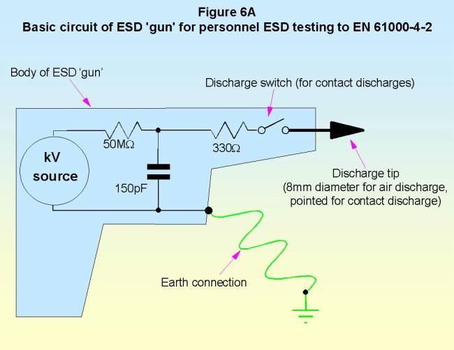
The ESD simulator used for testing to EN 61000-4-2 is based upon the 150pF/330W human body model, and generates a waveform with a risetime of between 700ps and 1ns to reach a peak of several kV, which then decays to about 50% in 50ns. At a voltage of 8kV the peak current into a 50W calibration load is close to 20A. The frequency content of such an ESD waveform is flat to around 300MHz before it begins to roll off, so contains significant energy at 1GHz and above.
Some older test standards use an older human body model which only has a 5ns risetime, so its spectrum begins to roll off at 60MHz and it is not as aggressive a test as EN 61000-4-2. As high-speed measurement techniques improve, it appears that real ESD events may have risetimes faster than 700ps.
Testing to EN61000-4-2 (personnel discharge) involves the following:
· Air discharges of up to ±8kV (using an 8mm round tip to simulate a human finger) are applied to everything non-metallic which is normally accessible to the operator.
· Contact discharges of up to ±4kV (using a sharp tip which is touched against the product before the discharge) are applied to operator-accessible metal parts – and also to nearby vertical and horizontal metal planes.
Test voltages are increased gradually from low values, often using the settings 25%, 50%, 75%, and then 100% of the test voltage. This is because ESD failures are sometimes seen to occur at lower voltages but not at the maximum test level. The highest test level on an ESD test is not necessarily the one most likely to cause a failure (this is also true for other types of transients). Figure 6A is a sketch of the barest essentials of an ESD ‘gun’.
Bear in mind that in dry climates personnel ESD events can easily exceed 8kV. 15kV or even 20kV is not that unusual during freezing winter conditions when the air is very dry, especially in heated homes and buildings without humidity control. So, meeting an ESD test at ±8kV is not a guarantee of freedom from actual ESD problems in the field, and the environment and needs of the users should be taken into account when ESD testing to help produce reliable products.
6.1.3 Design techniques for personnel ESD
All the design techniques described in the previous parts of this series help a great deal in improving the immunity of circuits to electric and magnetic fields, and so help circuits cope with the brief but intense bursts of wideband disturbances from ESD events. However, they are not usually enough on their own. The two main techniques for preventing ESD sparks from upsetting products are:
· Dielectric protection (insulation)
· Shielding (metal or metallised enclosures)
Dielectric protection is the preferred technique, but where it cannot be used for an entire product ESD problems can occur with both internal and external connections. These are discussed below. Apart from dielectric isolation, many of the techniques described below will also be useful for protection against other conducted transients and surges, which have not been dealt with in this series of articles as a separate topic.
6.1.4 Dielectric protection
This is the best ESD protection method. By not allowing an ESD spark to occur at all, not only are sparks prevented from getting into sensitive circuitry, but no bursts of electric and magnetic fields occur either.
Plastic enclosures, membrane keyboards, plastic knobs and control shafts, plastic switch caps, plastic lenses, etc., are all pressed into service to insulate the product (especially the operator-interface areas and controls). A 1mm thickness of common plastics such as PVC, polyester, polycarbonate, or ABS, is usually more than adequate to protect from 8kV of ESD (check the breakdown voltage rating of the material in kV/mm of thickness). But since no practical enclosure is without seams, joints, and ventilation, the achievement of adequate creepage and clearance distances becomes very important. Creepage is the shortest path that a current would have to take if it ‘crept’ along all available surfaces to reach the vulnerable part, while clearance is the shortest path to the vulnerable part through air (metal parts encountered along the way counting for zero distance regardless of their dimensions).
Clearance is the easiest to deal with, because the breakdown voltage of air is usually around 1kV/mm. So as long as the distance from the tip of the ESD gun to the vulnerable part is at least 8mm (preferably 10 or 12mm to give a design margin) an ESD spark can’t occur.
Creepage is more difficult, because the surfaces of plastics are always contaminated with mould-release chemicals, fingerprints, dust, etc., which attract moisture from the air and form a variable conductivity surface. Sparks from the tips of ESD guns are often seen to follow a random path over the surfaces of plastic enclosures, displays, keyboards, etc., sometimes for as long as 50mm as they follow the path of least resistance through the dirt on the surface of the plastic, eventually ending on a metal part. (Painted metal surfaces often show similar long random spark tracking, usually leading to a pinhole defect in the paint that it takes a microscope to see.) So it is very difficult to specify an adequate creepage distance which will protect from an ESD test, although more than 50mm is probably adequate except for polluted or wet environments.
Figure 6B shows a combined creepage and clearance design issue. A joint in a plastic enclosure could allow an ESD spark to travel along the surfaces of the plastic, then through the air inside the enclosure to terminate on a vulnerable PCB track. Figure 6B shows that it is usually a good idea not to line up PCBs with seams or joints in their plastic enclosure.

LCD displays, membrane panels, and tactile rubber keypads can be very good at preventing ESD if a few basic precautions are taken. Although their surfaces are ESD-proof at least to 15kV, they can have problems at their edges. ESD sparks can track along the dirt on their insulating surfaces, and go around their edges to reach vulnerable internal tracks.
LCDs often dealt with this problem by using large bezels which prevented fingers from getting too close to their edges. Insulating sealant and similar materials are now more likely to be used these days. Another method is to surround the LCD panel with a metal bracket that ‘catches’ the spark before it gets to any sensitive parts, but then something has to be done to remove the charge from the metal surround without it discharging itself into some sensitive part.
Membrane keypads and panels have internal conductive tracks, sandwiched between glued layers of plastic. If these tracks get too close to the edge of the panel, and if the glue has an airgap in it, sparks can track from the front surface (where the air discharge tip is applied), around the edge, through the void in the glue, and into the internal track, giving a false keypress if nothing worse. So whilst all attempts should be made to ensure there are no voids in the glue, it is still best to keep internal tracks at least 12mm from the edge of the panel (much more if possible).
Tactile rubber keypads also suffer from sparks that track through their surface dirt around the edges of their rubber mouldings and into the vulnerable keypad tracks behind. Unlike membrane panels, they usually don’t have the benefit of glue to provide insulation, so it is important to extend the rubber edges of the tactile key moulding for far enough out, whilst keeping the tracks on the underlying PCB far enough in, so that any sparks have too far to go.
When a plastic enclosure has an internal shielding coating applied to meet RF emissions or immunity requirements, this can compromise dielectric isolation measures. For the conductive layers to make a connection across enclosure seams they must extend at least a little way into the seams, and may even be fitted with a conductive gasket. This can compromise the creepage and clearance distances that had existed on the unshielded version, and ESD tests on such enclosures often find that when the tip of the ESD gun gets anywhere near seams and joints in the enclosure, a spark flies from the tip and disappears into the seam or joint to meet the internal shielding layer. In this situation it is usually very hard to achieve dielectric isolation for the whole enclosure, and the shielding method described next may have to be employed instead. Where possible it is a good idea to plan ahead so that plastic cases are designed to allow internal shielding to be added later without compromising the dielectric isolation ESD protection. This can be difficult to achieve, especially on small products.
6.1.5 Shielding
Shielding attempts to divert the (very large) ESD currents away from internal circuitry. In general it is not as good as dielectric isolation because it exposes all the external conductive connections (and possibly internal circuits too) to indirect ESD injection via ‘ground lift’.
When an ESD spark occurs to a metal enclosure, for the first few microseconds the enclosure will be at a much higher voltage than any protective earth it is connected to. This local ‘ground lift’ decays as the charge on the enclosure leaks away through the inductance of any protective earth connections (usually several tens of mH). Where an enclosure is not connected to protective earth the charge on the shielded enclosure leaks away slowly through ionisation currents in the air around it, conduction through humid fabrics, and similar mechanisms.
During the beginning of a ground-lift event, internal circuits may still be at their previous voltages and sparking may occur between the enclosure and internal parts. This is known as ‘secondary arcing’ and it can be as bad for semiconductors and signals as the original ESD spark.
As long as the internal circuitry can cope with the sudden change in potential of its enclosure they don’t care whether they are at protective earth potential, or 8kV relative to it. So it is quite practical to make battery powered or double-insulated products withstand ESD events (even though they are not connected to earth), although their isolation from earth may create greater problems for their external interconnections (discussed later).
So, on its own, having an external shield is not enough. One solution to secondary arcing is to bond the internal circuits to the enclosure shield, using connections that have a low enough inductance to maintain a low voltage between circuit and shield during an ESD event. These connections are often direct bonds from the 0V planes in the circuit boards to the enclosure, but they could be capacitive connections instead. Another solution is isolate the internal circuits from the enclosure using materials (or air spaces) that will not break down due to the voltage overstress.
Having dealt with secondary arcing we need to address the problem of transient current injection into the internal circuits.
The circuits within a shielded enclosure are all exposed to the internal fields created by the momentary ground-lift of the enclosure, before the internal potentials have had time to equalise. Because all the different PCB traces and components (even lead frames and bond wires) have different amounts of stray capacitance to the enclosure they each experience different amounts of injected stray current. Because the risetime of the ESD event is so fast and contains such a high frequency content, even very small stray capacitances can inject quite large currents. These different currents can create differential signals which can upset circuit operation. Figure 6C tries to show how this problem occurs.
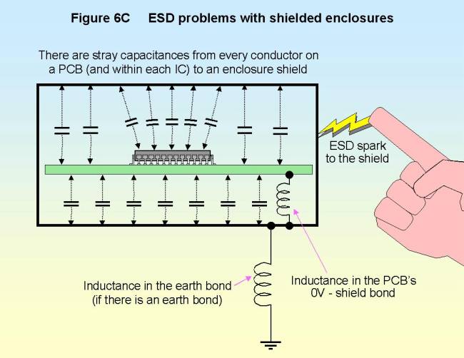
Solutions to the transient current injection include:
· Bonding the PCB ground plane(s) to the enclosure at very frequent intervals, to reduce the bonding inductance so that the ESD voltages equalise as quickly as possible. Quicker equalisation = lower internal voltage differences = lower values of transient current injection.
· Shielding sensitive circuits or ICs with PCB-mounted metal boxes bonded to the local PCB ground plane. These may be thought of as intercepting the stray capacitances from the components and PCB traces to the enclosure, diverting their transient currents into the ground plane where they will do less harm.
The problem illustrated by Figure 6C is often made worse where an enclosure contains a number of interconnected PCBs, as it is so difficult to ensure that during an ESD event they all charge up to the enclosure voltage at the same rate. If one circuit board has a low inductance connection to the enclosure, whilst another has a high inductance connection, then there can be a substantial transient voltage difference between them. This would inject a pulse of current into the boards’ interconnections, causing cause signal corruption if not actual damage. So it is always a good idea to bond the 0V planes in different boards together using a number of conductors (one reference conductor for every one or two signal conductors may not be excessive) to help prevent large internal voltage differences.
Where galvanic isolation of circuits from their enclosure is used to protect sensitive signals from differences in earth potentials, usually where long external cables are involved, the isolation is usually only needed at mains frequencies so it is often possible to capacitively bond across the galvanic barrier (with suitably rated capacitors). This equalises transient voltages during an ESD event without compromising functionality. Where this method is unsuitable, an internal shield over the isolated circuitry, bonded to its local isolated reference plane, may be required.
Even tiny gaps or joints in enclosure shields are weak spots, because they divert the very large fast currents from the ESD spark as they flow around the enclosure, causing locally intense pulses of electric and magnetic fields to be emitted through the shield and into the enclosure. Looked at from the frequency domain, we would say instead that the high frequency components of the ESD event find gaps and joints useful as slot antennae, radiating into the enclosure. So it is important to keep all gaps and joints in shields to a minimum size, as described in Part 4 of this series. Even if they are very small, sensitive circuitry should be kept well away from them.
6.1.6 Adding impedance to signal lines
Some interface devices (such as some RS232 ICs) are claimed to withstand EN61000-4-2 testing directly on their RX and TX connections. But for the vast majority of semiconductors it is by far the best to protect them from the direct effects of ESD by using the dielectric isolation (insulation) or shielding techniques, described above.
But if for some reason circuit conductors really must be exposed to ESD sparks: using a series resistor or choke (as shown in Figure 6D) may allow the ESD injection into the circuit to be handled by an IC’s own internal protection devices. This is only likely to be possible for interface or ‘glue logic’ devices, and can’t be generally recommended for VLSI devices such as microprocessors not intended to connect directly to external cables.

Most resistors or chokes aren’t rated for ESD voltages, but may cope if they are physically large, have enough thermal inertia, and don’t arc-over themselves. Since there is very little energy in a personnel ESD event, a large thermal inertia will prevent the resistor from suffering damage, although the same may not be able to be said of some machine ESD events involving large stored charge. It may be necessary to put a number of resistors or ferrites in series so that they share the ESD voltage and don’t arc-over or break down (close to each other and arranged in a straight line, to get maximum advantage from this technique).
Since resistor and choke manufacturers don’t specify their products’ specifications on EN 61000-4-2 tests, it is best to check a few in a representative circuit and PCB layout. It may be found that different values may be needed for different ICs. The chokes used should be carefully chosen to provide a high impedance over the range of frequencies encompassed by the ESD event. Always perform a number of tests, to make sure that ‘soft’ failures aren’t happening.
Mask shrinks by semiconductor manufacturers can make such a protective circuit design inadequate (just as it can invalidate all other EMC measures), so it is always best to have an arrangement with your semiconductor suppliers that they will warn you in plenty of time of any impending mask shrinks, so you can purchase some buffer stock to continue production whilst you evaluate all the EMC effects of the mask shrink, including any ESD protection.
The resistors or chokes may need to have such high values that they prevent the circuit from operating correctly. This is a particular problem for high-speed signals. One solution is to add discrete transient voltage suppressers, as described later. These will handle much larger voltage and current transients than most devices’ internal protection measures, allowing series resistors or chokes to be reduced in impedance, or removed altogether.
However, a potentially serious problem for all methods that merely prevent fatal damage to semiconductors from direct ESD injection, is that they do not prevent momentary corruption of signals. Signal corruption can cause an ESD test to be failed, even though devices are undamaged. This is discussed later.
6.1.7 Transient Voltage Suppressors (TVSs)
As asserted above, it is always best not to allow sparks to get into circuit conductors. But if, for some reason, circuit conductors really must be exposed to ESD sparks: it may be possible to arrange for the associated ICs to survive by fitting series resistors or chokes as described above. An alternative technique that is widely advertised by TVS manufacturers is to fit suitably-rated discrete TVSs between the vulnerable conductors and the local 0V plane, a shown in Figure 6D. Being very much higher rated than an IC’s internal protection devices, series resistance or chokes can have much lower impedance, and are often dispensed with altogether, which is sometimes much better for functionality.
Low inductance plane bonds are required for TVSs to protect ICs correctly, so the techniques described in Part 5 for connecting decoupling capacitors to 0V planes should be followed. Also, the PCB track to be protected must pass through the other terminal of the TVS. ‘Spurring’ a track from the signal path to a nearby TVS creates inductance which can prevent the TVS from protecting the IC. Since the TVS is required to bypass the powerful discharge current from the signal conductor into its local 0V plane, care must be taken that the ESD transient discharge current – now flowing in the 0V circuit and looking for a route back to the external earth – does not cause problems elsewhere in the product.
TVS components are now available in a wide range of voltage and power ratings, in leaded and SMD styles. They are also available as space-saving PCB-mounted arrays, and also fitted into connectors where they shunt the spark current into the metal body of the connector (which therefore needs to have a good high-frequency bond to the metal enclosure or the PCB’s 0V plane). Some manufacturers make very thin flexible circuits which fit over the solder pins of common connector types, allowing an easy TVS retrofit to every pin of the connector.
A big advantage of discrete TVSs over filtering is that they do not compromise high-speed signals as much. Most of them are based on zener technology so they do have some capacitance, and for very high speed signals the choice of an adequately low-capacitance TVS which still has the desired ratings can still be quite limited. Where extremely low capacitance ESD protection is needed, reverse-biased diodes between the signal conductor and the 0V and power planes, as shown in Figure 6E, can be effective. Reverse-biased diodes have a significantly lower capacitance than zener diodes. The diodes need to be able to handle the ESD currents when forward-biased, and the local power plane needs sufficient high-frequency decoupling capacitance so that its voltage does not rise too much when it absorbs the ESD charge. Where the leakage currents of TVSs or diodes are the problem, rather than capacitance, it is possible to use FETs instead to get nanoamp leakage.

Unfortunately, although TVSs are often advertised as a complete solution to problems of EN 61000-4-2 ESD sparks getting into exposed circuitry, this is not the case in practice. Their problem, which they share with the ICs internal protection devices and the reverse-biased diodes above, is that they cannot prevent the ESD transient from corrupting the signals on the conductors they are protecting.
Techniques additional to the use of TVSs are thus required to prevent signal corruption, and these are described in a later section.
6.1.8 Low-pass filtering the signal lines
Following a series resistor or choke with a capacitor to the local 0V plane (as shown by Figure 6F) can provide excellent protection from direct ESD injection to a conductor. As well as helping prevent actual damage, it can reduce transient voltages to such low levels that excessive signal corruption is prevented. Unfortunately, this approach has its limitations for high-speed signals.

The capacitor in the circuit shares the charge with the capacitance in the source of the ESD event. Since the source of a personnel ESD event has a capacitance of 150pF (although some older human-body models used by older test standards use 330pF) a 1nF capacitor in the circuit would reduce an 8kV voltage to about 1000V, 10nF would reduce it to about 120V, and 100nF would reduce it to about 12V.
Adding a series impedance such as a resistor or choke between the ESD event and the capacitor reduces the peak currents, which if left unchecked could be tens of amps and could physically overstress the capacitor and might also cause secondary problems due to the intense magnetic fields resulting. A 1kW series resistor would limit the peak current of an 8kV discharge to 8A, 10kW to 800mA, and 100kW to 80mA.
So we can see that a 100kW resistor followed by a 100nF capacitor would tame a personnel ESD event very considerably, where the wanted signals concerned were slow enough not to mind a filter with a 1 second time-constant. Of course, the series resistor or choke would need to be able to withstand 8kV without damage, and this rules out the use of ordinary resistors (unless a number are used in series). Surge-rated resistors are available, but they are larger and more expensive than ordinary resistors. Some manufacturers of ferrite beads test their products to check that they are not damaged when ESD events of up to 25kV are applied across them, but I am not sure whether they allow them to flash-over during the test. Surface-mounted resistors and ferrite beads may be relied upon to flash-over at quite low voltages, due to the small spacings between their terminations. Unfortunately a number of SMDs in series may not voltage-share very well due to variations in surface contamination, so when using this technique rather than a guaranteed non-flash-over (probably leaded) component – it may be best to design-in a very large margin (e.g. use twice as many components in series as appears necessary).
When the load impedance is much greater than the series impedance in the protection circuit, the high voltages due to the ESD event can last a long time and the protection is achieved by charge balancing and peak current limitation. But when the load impedance of the IC or circuit to be protected is much lower than the impedance of the series resistor of ferrite in the RC circuit, the ESD event lasts a much short time and so the RC circuit also acts as a low-pass filter, giving even greater attenuation of the ESD event and hence greater protection.
Applying the ‘low-pass filter’ protection circuit after a TVS (as shown in figure 6E) can be useful where load impedances are less than the impedance of the series element (resistor or ferrite choke): the TVS reduces the ESD’s 8kV (or whatever) to a few tens of volts, and the low-pass filter then attenuates it to less than the desired level. Of course, the peak currents into the TVS will be very large (unless limited by a series resistor) and these may cause problems due to their local magnetic fields, but the resistor or ferrite choke following the TVS will not have to be rated for the ESD voltage and can be an ordinary component.
Where fast signals are involved, filtering on individual lines may not be able to achieve useful ESD protection without negatively affecting the wanted signal, although common-mode filtering may well be possible (see later). Transient voltage suppressers may need to be used instead (see above), since they add only little capacitive loading, along with communication protocols or software techniques (see below), but it is still best not to let the spark get into the conductors in the first place.
6.1.9 Common-mode filtering at connectors
Because external signal and power cables are initially at their previous voltages, a ‘ground lift’ event due to a metal enclosure being struck by an ESD spark makes a transient high voltage appear across circuitry which interfaces with external cables.
All things being relative, it is as if the enclosure was at earth potential and all its external cables had been suddenly raised to a high voltage. For example, if an enclosure was suddenly charged to +4kV by an ESD spark, it is as if the enclosure remained at earth potential but all the external cables had been suddenly charged to -4kV instead.
Although filters and/or TVSs may be used on each individual power or signal line, to help protect the electronics interfacing with the external cables (as described in the previous two sections), filtering each signal line independently is usually not compatible with high-speed signals, whereas TVSs can’t prevent signal corruption (see later).
Because the transient voltage experienced by the interface circuitry is identical for all the conductors in a given cable it is a common-mode (CM) transient, and CM suppression techniques may be used to help suppress the transient voltage without compromising high-speed signals.
Figure 6G shows a common-mode choke used for this purpose. It needs as many windings as there are conductors in the cable. Surface-mounted and leaded common-mode chokes are available with up to eight windings. If the CM choke has a high enough value of common-mode impedance over the frequencies of concern it may be able to prevent an ESD transient from damaging the interface electronics. In situations where signal corruption is the problem, a CM choke can greatly reduce the signal perturbation.

When a CM choke is used with filter capacitors even greater suppression can be achieved, although this is not as suitable for high-speed signals unless quite small capacitor values are used (say between 10pF and 1nF, depending on the application).
Where a large number of conductors must be accommodated specially-wound chokes may be required. A favourite technique is to pass the cable through a soft-ferrite cylinder or toroid. A single pass through a typical 32mm long ferrite cylinder creates a common-mode impedance of around 250W at 100MHz, not as much as some PCB-mounted components, but often enough to make a useful improvement to an EMC problem.
Where higher common-mode impedance is required, two or more turns of the cable could be made through the ferrite, to increase the impedance. Unfortunately, multiple turns also reduces the frequency at which the peak impedance is achieved, so beyond a certain number of turns no further benefit (at a given frequency) may be achieved by adding more turns. We would normally expect that the impedance presented by a choke would increase according to the square of the number of turns, but this is not always the case for soft ferrites, as shown by the following example (kindly provided by Alan Keenan of Steward Inc.). Tests on a particular soft-ferrite core found that with two turns its Z peaked at 692W at 322MHz; with three turns its Z peaked higher at 809W but at the lower frequency of 152MHz; and with four turns wound on it - its Z peaked even higher at 1300W but at the even lower frequency of 108MHz.
Multiple ferrites strung along a cable increase impedance proportionally to the number of ferrites, without reducing the frequency of the impedance peak, but can look a bit Heath-Robinson. Cables passed through ferrites should always finish on the other side of the ferrite from the side they entered, so that the ferrites are like beads strung on a length of string, for best high-frequency performance. Any stray capacitance from one end of the ferrite (or chain of ferrites) to the other will compromise the high-frequency performance, making the routing of the cable or track very important.
6.1.10 Galvanic isolation techniques for ESD
Galvanically isolated external connections help a great deal with making products immune to ESD (and also to conducted transients and surges). PCB-mounted opto-isolators and transformers may be used, although many types will not have sufficient creepage and clearance and voltage withstand for ESD, and many types will have internal parasitic capacitances which may allow excessive transient currents to flow. Isolating mains transformers that meet their appropriate safety standards often seem quite adequate for protecting power supplies from personnel ESD, despite their shortcomings as ESD barriers.
The very best galvanic isolation for external signal communications is achieved with fibre-optic, wireless, or infra-red techniques, since these do not involve any conductors with dissimilar voltages being anywhere near the product concerned. Of course, the transmitting and receiving modules concerned can be very sensitive, and are often best fitted with their own local shielding, but even quite large PCB-mounted shields are now available taped and reeled for automatic placement and so can be much more cost-effective than when such items required manual assembly. Fibre optic cables sometimes use metal strengtheners, armour, or metal vapour barriers, and these can compromise the creepage and clearance distances required for ESD protection so should be stripped well back from any connections with products, where it is not possible to avoid the use of such cables entirely.
Five years ago I began expressing the opinion that by 2005 people who used copper cables to connect signals between items of equipment would be thought rather old-fashioned, and I still believe that this timescale is correct.
6.1.11 Dealing with signal corruption
When ESD testing to harmonised EMC standards using the EN 61000-4-2 test method, it is normal for the requirement to be that the operational state of the product being tested (and its displays and stored data) is exactly the same after the test as before. This is usually also the case for other transient tests such as Fast Transient Bursts (EN 61000-4-4), Surge (EN 61000-4-5), and the various automotive transients described by ISO 7637.
Using an IC’s internal protection or a TVS to protect against ESD (or other types of conducted transient or surge) does nothing to prevent signal or data corruption, and can result in the product’s operational state, displays, or memory being different after the test, leading to test failure. Additional techniques are often needed to prevent signal corruption.
For ordinary control lines such as keyboards, ‘debouncing’ techniques (whether hardware or software, such as are routinely used to debounce mechanical contacts) can work very well. Low-pass filtering (see above) is a good old-fashioned ‘debouncing’ technique often used after a TVS.
High-speed data can’t use powerful debouncing techniques, and some type of error-protecting protocol is usually required, although of course this slows down the data rate too.
Where a single ESD event causes a single bit error in a serial communication, the use of simple parity check or Hamming coding can make a big improvement in immunity. However, these techniques will be less effective when the interference comes in bursts, as is usual for non-ESD transients, or when an ESD event causes secondary arcing. Some very comprehensive error-correcting protocols are now commercially available (see section 1.4.7), and it is usually much more cost-effective and time-saving to purchase the necessary chips or software licenses than it is to try to develop your own protocols. Unlike simple techniques such as parity checking or Hamming coding most such protocols have a high resistance for burst errors, and have been field proven in a wide range of applications and situations.
Momentary corruption of analogue signals is sometimes acceptable, when all that results is a brief click in a headphone or momentary flicker of a meter needle. But where decision thresholds may be crossed, or where the analogue signal is put through an averaging routine or stored in a memory after digitisation, even a brief error in an analogue signal may be unacceptable.
Since analogue signals can’t easily use error-correcting protocols, debouncing techniques (such as a low-pass filter) are often used. Where the analogue signal must use high frequencies, it becomes very difficult to filter the transient event from the signal, the more so as the accuracy required (equivalent to number of bits of resolution) is increased, so dielectric isolation or shielding techniques are necessary after all, to prevent the ESD transient from getting into the signal conductor.
6.2 Dips, sags, brownouts, swells, dropouts, interruptions and power outages
According to some experts, the effects of poor supply quality on electronic equipment is one of the most significant causes of downtime and financial loss world-wide. Dips, sags, brownouts, swells, voltage variations, dropouts and interruptions are the main causes of poor supply quality. (In some areas waveform distortion is also becoming an important issue.)
EN 61000-4-11 is the basic test standard for dips, sags, brownouts, swells, voltage variations, dropouts and interruptions in the AC mains supply, but is not harmonised under the EMC directive so cannot be used when self-declaring conformity to standards. For self-declaration to standards it is necessary to use the harmonised generic or product standards - which now generally call-up the use of EN 61000-4-11 as the basic test method. It is always the generic or product standards that set the actual test limits, and they are often a lot less comprehensive than the limits in EN 61000-4-11.
When using the Technical Construction File route to conformity it is often permissible to use EN 61000-4-11 directly.
Of course there is no reason why a manufacturer should not apply EN 61000-4-11 to a product in any case, in addition to the requirements of any harmonised product or generic standards, and this may sometimes discover reliability problems with products that would otherwise have been overlooked.
Dips are short-term reductions in supply voltage caused by load switching and fault clearance in the AC supply network. They can also be caused by switching between the mains and alternative supplies in uninterruptible power supplies or emergency power back-up systems. Examples of dips: 30% dip for 10ms, 60% dip for 100ms. Figure 6H shows a 40% dip for 20ms (one mains cycle). A dip of 40% is equivalent to a reduction in supply voltage to 60% of its nominal value.

EN / IEC 61000-4-11 refers to a Unipede study of dips which covered public mains supplies.
Dip depth Number of dips/yr with given durations
10-100ms 100-500ms 0.5-1s 1-3s
10-30% 61 66 12 6
30-60% 8 36 4 1
60-100% 2 17 3 2
Dips may not occur in isolation - sometimes a fast sequence of dips occurs. Most immunity tests apply dips abruptly, starting and finishing at a zero crossing, but in practice they can have gentle rates of change and start and stop at any point in the mains cycle.
EN61000-4-11 recommends testing with 30% and 60% dips (70% and 40% of nominal voltage respectively) for 0.5, 1, 5, 10, 25 and 50 cycles of the supply waveform in each case. Although the generic immunity standard for domestic, commercial, and light industrial environments EN 50082-1:1997 (which will be replaced by EN 61000-6-1 sometime around 2004) uses EN 61000-4-11 as its basic test method, it merely requires testing with 30% dips for 10ms and 60% dips for 100ms.
Likewise, EN 61000-6-2:1999 (which replaces EN 50082-2:1995 in April 2002) also uses EN 61000-4-11 as its basic test method but only requires testing with 30% dips for 10ms, 60% dips for 100ms and 1 second. Many of the other harmonised standards under the EMC and RTTE directives specify dip test % and durations which are different from the above generics and from each other, and which are not as comprehensive as EN 61000-4-11.
Because no high frequencies are involved it is fairly easy to construct your own supply dips tester using a pair of solid-state zero-crossing relays, a variable transformer and a timing generator, as shown by Figure 6J. Safety issues must not be neglected ! A test laboratory would be more likely to use a programmable mains synthesiser with enough short-term capacity to handle the product’s inrush current.

Sags, swells, and brownouts are slowly-varying changes in voltage, sometimes over periods of hours. They are sometimes called ‘voltage variations’ and some people don’t consider them to have anything to do with EMC. A brownout is another name for a sag, and is a term most often heard in the USA and Canada. Sags and brownouts can go right down to zero volts. Swells are simply slow increases in voltage, as opposed to surges and transients, which are fast increases.
Typical mains supplies are specified at ±6% voltage tolerance (sometimes ±10%) and it is not unusual to experience these ranges daily. Safety tests apply ±15% for long periods of time, so voltages of these levels are clearly not impossible. It is often claimed that European mains supplies don’t suffer from the traditional ‘brownout’ where the voltage falls by a large amount for minutes or even hours – but 60% nominal voltage for an hour or two every weekday is known to occur in parts of Spain – and 50% nominal for 8 hours has been measured by the author in the UK.
A sagging supply voltage is a particular problem for all AC motors and some types of DC motor because they can stall, overheat, and damage their insulation. This can lead to an increased risk of fire, fumes and electric shock, never mind the damage to the equipment. In industrial plant AC motors are usually protected by undervoltage trips which are usually incorporated with other protective functions into motor control circuit breakers devices (MCCBs).
EN 61000-4-11:1994 suggests testing with 40% supply voltage for 1 second and also 0% supply for 1 second with the supply voltage ramped down and then up again over a period of 2 seconds in each case. It does not suggest testing for swells despite the fact that these can damage surge suppression devices.
Surge suppression devices are often designed to operate as close to the maximum expected mains voltage as possible, to protect the equipment better. But their leakage at voltages above nominal can cause overheating and damage if the higher voltages last for more than a few seconds. Maybe EN 61000-4-11 assumes that safety testing would discover such problems.
Most (if not all) harmonised generic and product standards don’t specify any testing at all for sags, brownouts or swells. Testing to EN 61000-4-11 may be a good way to improve product reliability in the field. It may also be a good idea to test for anticipated swells, although EN 61000-4-11 doesn’t recommend any test levels.
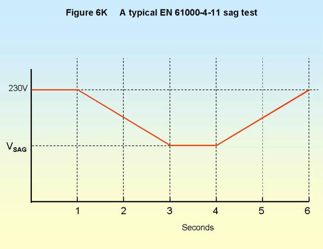
Figure 6K shows the voltage versus time profile for a typical sag or brownout test to 50% nominal voltage (in this case). It can easily be done manually by simply using a variable transformer (‘Variac’), although a test laboratory would be more likely to use a programmable mains synthesiser with enough short-term capacity to handle the product’s inrush current.
In real life brownouts can last for minutes at a time (8 hours at 50% voltage was once seen in the UK) so where motors or other vulnerable parts are concerned it may be best to test for a longer time than merely 1 second to ensure reliable operation in the field.
Swell testing can also use a variable transformer and manual control. A test laboratory would be more likely to use a programmable mains synthesiser with enough short-term capacity to handle the product’s inrush current.
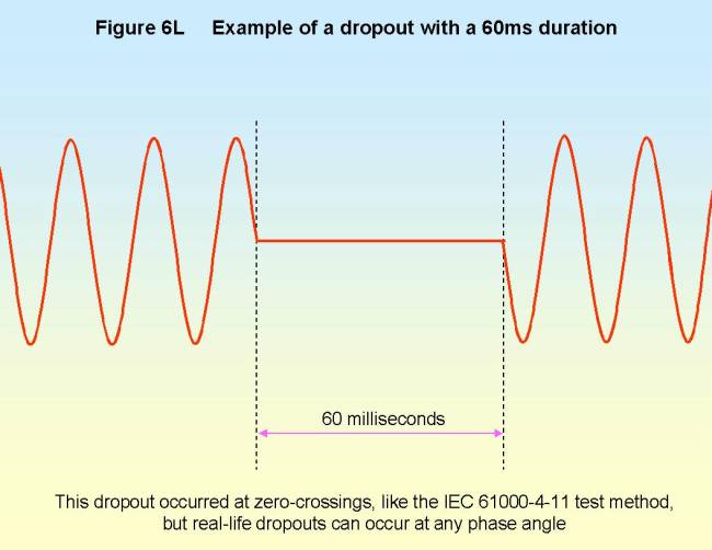
Dropouts are short-term 100% reductions in supply voltage (effectively 100% dips). Figure 6L shows a dropout 60ms long (3 mains cycles). Like dips, they are caused by load switching and fault clearance. Also like dips, they can be caused by switching between mains and alternative supply in uninterruptible power supplies or emergency power back-up systems.
EN 61000-4-11 refers to a Unipede study of public mains supplies which recorded 12 dropouts per year with durations lasting between 100 and 500ms, and suggests testing with dropouts lasting for 0.5, 1, 5, 10 supply cycles.
But EN 50082-1:1997 (EN 61000-6-1 from 2004) and EN 61000-6-2:1999 (replaces EN 50082-2:1995 in April 2002) don’t specify any dropout testing at all. It is clearly possible to declare EMC conformity without testing for dropouts, but your products might not be as reliable in the field as you would like. It is easy to make your own dropout tester using the method described for the dips tester but setting the alternative supply to zero.
Interruptions are supply voltage dropouts (= 100% dips) that last for a long time: seconds, minutes, or hours. They are really power outages. As for dips and interruptions, it is easy to make your own test equipment.
EN 61000-4-11 refers to a Unipede study of public mains supplies that showed...
Interruptions lasting: 0.5-1s 1-3s >3s
Number of interruptions/year: 24 5 0
(How did they manage to find no interruptions lasting more than 3 seconds? This doesn’t agree with many people’s experiences of UK mains supplies.)
EN 61000-4-11 suggests testing with interruptions lasting 0.5, 1, 5, 10, 25, and 50 supply cycles. But EN 50082-1:1997 (replaced by EN 61000-6-1 in 2004) and EN 61000-6-2:1999 (replaces EN 50082-2:1995 in April 2002) both specify testing with interruptions of 5 seconds duration only (= 250 cycles).
Equipment which has been designed to pass a 5 second power outage test might fail a 1 second outage test, so testing with all the durations suggested by EN 61000-4-11 might be a good idea to increase product reliability.
Waveform distortion is an increasing problem due to the proliferation of electronic loads on the power networks. 4% is getting to be the typical total harmonic distortion of European mains supplies, and this reach 8% in a few years. Most of the distortion consists of ‘flat-topping’, which means that the mains’ peak voltage can be much lower than Ö2 times its RMS value.
In parts of China the mains can be an actual square wave. As Figure 6M shows, parts of Israel also suffer from significant waveform distortion and this is probably not untypical of a number of countries around the world. So although a meter might read 230Vrms, rectifier-capacitor power supplies could give as little as 75% output before any supply voltage tolerances are considered.

Privately-generated mains supplies can be much worse than the normal mains, although in the ’Internet Hotels’ which now host so many of our web sites the mains supplies can be very much better (they need to be - a typical ‘Cisco hotel’ has an availability specification of 99.9999% and a power consumption of around 10MW).
An oil exploration platform had a 230V mains supply with a tolerance of ±100% caused by the effects of starting and stopping its huge drilling motor on its diesel generator. The voltage variations would last for several seconds each. Emergency 230/400V mains generators can have output quality much worse than a typical public mains supply, and much worse than the suggested test limits in EN 61000-4-11. So if your product is likely to be operated on a private mains supply, it is best to always find out what it is likely to be exposed to!
It is often thought that electro-mechanical components such as relays, contactors and solenoids are immune from EMC considerations. Certainly the designers of so-called hard-wired safety systems seem to believe this untruth. In fact dips, sags, brownouts, dropouts and interruptions can cause energised relays and contactors to ‘drop out’ and solenoids to lose power and move.
Although most designers would presumably consider the effects of a power outage (interruption) they would probably not consider a momentary dip in the supply that might cause some types of relays to drop out while other types remain energised. This situation is made more complicated because the ‘pull-in’ (must operate) and ‘drop out’ (minimum hold-in) voltages of relays and contactors rise significantly as they age.
Sometimes relays, contactors, solenoids, etc. are ‘held in’ at a reduced voltage, to save power consumption, and so might not pull back in again when the supply recovers. So we can see that ‘relay logic’ might not recover to its original state after the dip, dropout, sag, or interruption; and during the event itself they might operate in an unpredicted manner. Few designers of industrial automation seems to design or test for these problems, even though dips and dropouts are considered by experts to be a a major cause of lost production world-wide. (Few also seem aware of the fact that supply surges can arc unpredictably across mechanical contacts, also causing unpredictable operation of ‘relay logic’ systems.)
Figure 6N shows a typical problem for electronic circuits – the logic supply voltage going out of tolerance due to a momentary dip or dropout. The example is of a 40% dip for 40ms (two cycles of the supply), and shows how the unregulated DC rail droops to below the 5V regulator’s drop-out voltage during the dip. The 5V supply to the logic ICs thus falls out of regulation and can fall outside of the tolerance band required for correct logical operation of the ICs.

During this out of tolerance period anything can happen to logic systems and any software they are running - it is a very unpredictable situation and the results can be very damaging to product functionality. Operational malfunctions may be expected and it is not unknown for areas of memory to be wiped or over-written with garbage.
Because most designers only provide the minimum amount of energy storage on the unregulated side, many modern products are vulnerable to this problem. It is often found that products which are quite immune to their mains supply being switched on and off are vulnerable to dips and dropouts lasting just a few tens of milliseconds. It is difficult to manually switch mains faster than 200ms, while surveys (such as Unipede’s) show that shorter dips and dropouts are more commonplace.
Immunity to dips, flicker, and dropouts is usually easiest to achieve by making sure that the unregulated DC rails of a product’s power supply have long enough ‘hold-up’ times. This is usually achieved by using higher values of capacitance on the unregulated DC rail and also by increasing the unregulated voltage so as to allow for the increased DC ripple during the dips and dropouts. We need sufficient energy storage, given the power consumption of the product, to ride through the frequent short dips and dropouts. If non-essential functions can be switched off during a ‘hold up’ event, or microprocessors put into ‘sleep’ mode, it will help increase ‘hold-up’ time.
When dips or dropouts last so long that they become sags, brownouts, or interruptions and the unregulated energy storage cannot ‘hold-up’ any longer, it is important to ensure that before the logic (or other) DC supplies go out of tolerance the product ‘cleanly’ and safely ceases operation and shuts down. Then, when the event has passed, ‘cleanly’ and safely restoring operation (see later for more on the safety issues associated with power restoration). (In this context ‘cleanly’ means that no unintended operations occur and no memory is lost or corrupted.)
Figure 6P shows that because capacitive energy storage (in Joules) = ½CV2, for two identical CV products the energy storage of the higher voltage part is greater. CV product is closely related to physical volume and cost, so the two capacitors in the example will have the same physical size and cost despite the higher voltage one holding twice the energy. Note that to use a much higher unregulated voltage usually requires appropriate circuit design for the regulator so that the higher voltage can be efficiently utilised.

Continuous operation from a battery which is usually being charged up by mains-powered charger, as is normal for portable computers, is an excellent way of overcoming all dips, sags, dropouts; and interruptions lasting from minutes to hours (even months in some cases).
Most mains power supplies use unregulated DC rail voltages that exceed the dropout voltage of their regulators by the minimum amount possible, to improve efficiency and reduce size and cost. Unfortunately, this makes it difficult for the unregulated storage to provide much protection against dips and dropouts. (In the section on emissions of voltage fluctuations it is also shown that such designs make some products more likely to have emissions problems.)
Using unregulated DC rails with an increased voltage makes it easier to achieve significant energy storage to cope with dips and dropouts at reasonable cost, because capacitors store more energy per unit volume at higher voltages, as described earlier.
Operating the unregulated DC storage at a much higher voltage than is needed for circuit operation makes it possible for all the excess voltage to be used for DC ripple caused by dips and dropouts. When linear regulation is used higher unregulated voltages make efficiency worse, so this method is more suited to switch-mode regulators (which will probably need higher voltage ratings for their power devices).
Where an ‘Active PFC’ or similar boost converter precedes the unregulated DC storage capacitor (refer to the section on harmonic emissions) – designing the boost converter for a wide range of input voltages can ensure that the unregulated DC rail is kept fully charged even during quite severe dips and sags. A standard ‘universal input’ power supply (80 - 260V) used on 230V mains will be happy to operate continuously with only 80Vrms input, equivalent to a 65% dip or sag lasting for any length of time.
But ‘universal input’ power supplies won’t protect from dips and sags of more than 30% when used on 110V mains. To protect from larger dips and sags they would need to be re-designed for a 40 - 130V range. Alternatively they could be preceded by a selectable (110/230) voltage-doubler type rectifier circuit. In both these cases the benefit of ‘universal’ operation is lost unless the switch from 115 to 230V operation is done automatically.
Some products with linear power supplies have used triac-tap-switched mains transformers for many years. The triacs are switched automatically between a number of tappings on the primary of the transformer, to maintain the secondary AC voltage (and the unregulated DC voltage) within limits during dips, sags and swells. Hysteresis is used to prevent the triacs from ‘hunting’ between taps when the sensed voltage is close to a switching threshold. The unregulated DC needs to have enough hold-up for the response time of the tap-changer.
No boost converter or tap-changer can cope with a dropout or interruption – but at least they can help a little by making sure the unregulated DC capacitors are fully charged when the dropout begins. This won’t make any difference on formal EMC tests, but it may make a useful difference in real life, where dropouts can follow immediately on from a dip or a sag (brownout).
Designing equipment to cope with swells can just be a matter of rating components to cope with the overvoltage, and maybe with some extra heating too. Alternatively, it is possible to detect a dangerous overvoltage and shut down the equipment to protect it – although this should only be done where the user can cope with the resulting non-availability and no safety hazards are caused.
Surge protection devices (SPDs) are usually dimensioned to start conducting at just above normal mains tolerances. A swell which is higher than these tolerances could easily burn them out, since they aren’t rated for continuous dissipation. Some SPD types fail short-circuit and cause the equipment’s supply fuse to open, taking the equipment out of service. Some types fail open-circuit and can leave the equipment vulnerable to supply surges, with no warning. Overheating SPDs can cause fire and shock hazards if the designer has not considered the fact that they might glow red hot during a supply swell.
A number of ICs are now available for monitoring power supplies and effecting a controlled shut-down and reset when unregulated or regulated DC rails drop too low. These are usually sold as ‘brownout detectors’. Almost no equipment nowadays should rely on a simple resistor-capacitor-gate ‘power-on reset’ circuit, because they have always been inadequate for protecting circuits from the full range of perturbations of the AC supply.
Some power-monitoring devices monitor the unregulated rail so they are able to protect logic circuits before their DC rails goes out of tolerance by inhibiting read/write operations to memories of various types. This prevents memories from being overwritten with garbage during an undervoltage situation. In the case of brief events which don’t require a reset some devices can simply freeze RAM data momentarily enabling operation to continue as if no hiccup in the supply had ever happened.
Various grades of brownout detector are available, depending on the accuracy and tolerance of their voltage detecting functions. The more accurate and the tighter their tolerance, the more costly the tend to be. They are also available with a variety of functions to suit different applications.
Some circuits sample the mains voltage, usually to control heat or other parameters. These can often use a smoothing capacitor to ride out short-term disturbances. But some circuits take timing data from the mains, usually from the zero crossings. These can miscount, misfire, and go wrong in a number of ways – so their design must ensure that all foreseeable timing glitches are prevented or else don’t cause any malfunctions or damage.
The desired behaviour of equipment during supply dips, sags, swells, dropouts and interruptions depends on the application, and may be critical in safety-related applications. Some applications may need a controlled power-down, which may mean providing sufficient energy storage to manage the power down process. But some applications (e.g. medical life support) may not permit a power down at all, making their energy storage requirements very high.
Logic circuits should be prevented from causing malfunction by brownout detectors, but analogue circuits also need consideration. For example an audio amplifier must not produce loud instability, pops, clicks, or thumps during power down (or power up).
For motor drives the requirements depend strongly upon the application. They might be required to stop as quickly as possible, coast, or slow down in synchronism with a number of other motors controlled by other manufacturer’s equipment as a part of a large installation. When power is restored motors might need to ramp their speed up slowly or quickly, or they may not be allowed to rotate until manually commanded.
Since the EMC Directive does not cover safety, where errors and malfunctions in safety-related systems can be caused by the effects of electromagnetic disturbances on electronic circuits, these must be dealt with under safety directives such as the LVD or Machinery Directives.
Uninterruptible power supplies (UPSs) can be used to help products ‘ride through’ dips, sags, dropouts, and interruptions, but are not a universal panacea. Their ability to cope with all AC power EMC disturbances without passing them on to the ‘protected’ equipment should be investigated carefully, as should their reliability performance.
It has been known for the reliability of electronics to be reduced because the UPSs they were run from had lower reliability than the mains supply they were supposed to be improving on. Having said that, properly dimensioned and reliable UPSs which use full-time double-conversion can be a great help in preventing mains power quality problems from disturbing the operation of equipment.
Continuous double-conversion types are preferable as they don’t cause dips and dropouts by switching between their mains and alternative power sources. Many low-cost UPSs don’t use continuous double conversion and may not be able to respond to short dips and dropouts – indeed they may actually cause dips and dropouts by their mode of operation. These may be able to be used if the equipment’s power supply has sufficient hold-up time.
Some models of UPS provide good isolation from conducted RF interference, transients, surges, etc. – but not all of them do – so check the manufacturer’s specification carefully! Also make sure that the UPS will withstand the types of dips, sags, swells, and dropouts that you anticipate for the application. Some UPSs do not themselves have low levels of harmonic emissions into their mains supply, and some might supply distorted output waveforms (including rotary types such as motor-generator sets).
Serious energy storage may be needed if equipment is to keep functioning during a long power outage. Where loads are light, batteries or ‘supercapacitors’ may provide sufficient energy for weeks, but at the other extreme serious power users may need rooms full of batteries just to keep them going for the 30 seconds or so it takes their diesel-powered generators to get up to speed.
One way of reducing energy storage needs and getting increased operational time from your energy storage is to shut down non-essential functions during an outage. Some lighting, heating, chilling, and some visual displays may be able to be treated as non-essential.
Some types of UPSs only support and preserve the mains waveform, rather than take over from the mains. A paper mill in South Africa uses a superconducting energy ring in such a UPS to provide enough storage just for dips and dropouts. At a cost US$10 million it cost less than the web-breaks they were getting every week.
Motor-generator sets with alternative power sources for the motor are the original continuous double-conversion UPS. Motor generator sets are also very useful for preventing harmonic emissions from getting into the public mains supply. If they have enough rotational inertia they can also help reduce the load current fluctuations that would otherwise cause emissions of voltage fluctuations and flicker.
Automatically controlled motorised variable transformers (variacs), ferroresonant constant voltage transformers (CVTs), etc. are all systematic ways of dealing with sags and swells.
6.3 Emissions of voltage fluctuations and flicker
EN 61000-3-3 assumes a typical value for mains supply impedance at 50Hz of (0.24 + j0.15) W for the phase conductors and (0.16 + j 0.1)W for the neutral. When testing single-phase equipment these two are combined into one overall source impedance of (0.4 = j 0.25)W, and it is worth noting that j0.25W at 50Hz corresponds to an inductance of 796mH. When testing balanced three-phase equipment which draws negligible neutral current the neutral impedance is neglected and the overall phase-to-phase impedance is (0.48 + j0.3)W.
When equipment draws a fluctuating current from its mains supply these impedances in the supply convert the fluctuating currents into fluctuating mains voltages, as shown by Figure 6Q. These can cause problems for other equipment and also cause lighting ‘flicker’. Lightning flicker is very annoying to most people and can reduce their working efficiency. In some cases flicker can cause actual illnesses (especially those related to stress and/or eyestrain) and it may be able to encourage epileptic fits in susceptible people.

EN 61000-3-3 is now mandatory under the EMC Directive for all equipment that consumes up to 16A/phase from the public 230V supply. Test laboratories use an instrument called a ‘flickermeter’ to measure to this standard. EN 61000-3-3 limits the emissions of voltage fluctuations and flicker and also limits the inrush current at equipment switch-on. The inrush current requirement arises because after a power outage the very heavy inrush currents typical of electronic equipment (as they recharge their DC storage capacitors directly from their bridge rectifiers) can cause an overcurrent trip to occur in the high-voltage distribution, making restarting the network very difficult.
In the case of momentary power outages caused by arc-suppression protection devices on high-voltage overhead power lines when a lightning strike occurs, an overcurrent trip when the power is re-applied can extend what was a two-second outage to one that could last several hours.
Because so much of the load on the low-voltage power network is now electronic apparatus, high-voltage overcurrent tripping due to inrush is now a serious problem and the inrush currents of apparatus need to be controlled. Unfortunately, the issues of EN 61000-3-3 which exist at the time of writing do not mention the reason for its inrush current limit, making it easy for designers and test laboratories to accidentally overlook this requirement.
The requirements of EN 61000-3-3 are very complex because they are based on human perceptions of lighting flicker. The limits for voltage fluctuations and flicker follow a curve of amplitude versus rate (figure 4 in EN 61000-3-3) intended to correspond to the human perception of lighting flicker on a 60W filament light bulb, and are shown in Figure 6R. The peak human sensitivity to flicker is between 5 and 20Hz (300 to 1200 fluctuations per minute) so these rates have the toughest limits. At lower or higher rates greater levels of voltage fluctuation are permitted. For instance: at a rate of once per minute, the permitted voltage fluctuation level is approximately 10 times higher than the limit for 1000 fluctuations per minute.

For voltage fluctuations that occur every 1.25 minutes, the steady-state limits for a step-change are 3% of the nominal voltage, corresponding to a change in resistive load current of 15A every two minutes or so. This allows typical domestic hotplates, heaters, etc., to be switched on and off without suppression as long as they don’t switch more often than once every 1.25 minutes.
The peak limit for a step-change fluctuation every 1.25 minutes is 4%, one-third higher than for steady-state value, equivalent to a resistive load current change of about 20A. The steady-state limit must not be exceeded for more than 200ms.
During an initial switch-on inrush situation, or for load-switching events that occur less than once per hour, the values of the steady-state and peak voltage fluctuations are allowed to be 33% higher than the above. It may be that future versions of EN 61000-3-3 will permit equipment that delays its switch-on inrush current by more than 10ms to have even higher emissions, since delayed inrush places less of a burden on a mains network which is being restarted after a power interruption.
The basic limit curve (figure 4 in EN 61000-3-3) assumes a simple step change in mains voltage (whether an increase or a decrease) – but different voltage fluctuation waveshapes cause different flicker perceptions. Some waveforms will measure lower or higher values for their peak voltage fluctuations than others, even if their instantaneous peak values are the same. A complex mathematical transformation is required to determine whether a non-step type of waveform complies with the limits. This transformation is conducted automatically by the digital signal processing in ‘flickermeters’ (for which the defining standard is EN 61000-4-15).
Section 4.2.3 of EN 61000-3-3 gives some guidelines to designers for estimating the effects of waveshape on peak voltage fluctuation for a few commonly-encountered shapes – but only for fluctuations that occur less than once per second. This makes it easier to estimate the likely voltage fluctuation emissions from an equipment calculation, simulation, or by simple measurements using standard laboratory equipment (oscilloscopes, for example). The accuracy of these estimates is claimed to be no better than ±10%, so results which are within 20% of a limit should be checked with a flickermeter on the actual equipment to make sure it complies.
If you are using a test supply with a total harmonic distortion of under 10% and a supply impedance the same as that specified by EN 61000-3-3 you can measure the voltage fluctuation directly with an oscilloscope. If instead you measure the load current fluctuation with another supply impedance you would need to transform it mathematically into the voltage fluctuation that could be expected using the standard impedance. But beware – the load current fluctuations will themselves depend upon the supply impedance, so if measuring load current it is best to make sure your supply impedance is close (both in resistance and inductance) to the standard supply impedance. Synthesised sources of mains voltage are now available, either with programmed impedances (or zero) achieved by feedback techniques or with the standard impedance. As time goes on more manufacturers are entering this market and the cost of these sources is falling. Figure 6S shows an example of such a source.

If you know your equipment’s load current waveshape – whether calculated, simulated, or measured with close to the standard source impedance – you can calculate or simulate the resulting mains voltage fluctuation waveshape. By referring to 4.2.3 and figures 5, 6 and 7 in EN 61000-3-3 you may find that altering the load current waveform can give useful reductions in the measured flicker value, even if the rate per minute, peak and steady-state amplitudes of the fluctuation remain unchanged.
EN 61000-3-3 requires the integration of each measured sample of voltage fluctuation for a period of 10 milliseconds. Voltage fluctuations occurring on shorter timescales are ‘smoothed out’ by this integration process.
6.4 The influence of the supply inductance
The supply impedance has an inductive component (L), so since V = Ldi/dt the rise/fall times of the load’s current waveform could have an effect on voltage fluctuations. The standard total single-phase L is around 796mH and its impedance exceeds the resistive component of the supply impedance above 80Hz. The rate of change of current required to create a 4% voltage fluctuation – due to the standard supply inductance alone – is 11,558 A/s.
80Hz is not a very high frequency, so equipment which draws fluctuating currents with spectral components above 80Hz may find that the inductive component of the standard supply impedance contributes more to the measured voltage fluctuation than the resistive component.
For example, high rates of current change are commonly exceeded by DC storage capacitors charging-up via rectifiers directly from the mains, especially when they are connected at the peak of the mains cycle – the worst-case for capacitor inrush. But under such conditions typical capacitors of under 1,000mF require less than 1ms to charge to 370V and although the peak voltage fluctuation caused by the capacitive inrush would be very large indeed, the 10ms integration time ‘smooths it out’ to make the EN 61000-3-3 measured value very much less. Simplified analyses indicate that the rectifier-capacitor power supply input stages typical of switch-mode power supplies risk failing the inrush current limit when capacitor values exceed 600mF.
Where the DC current load on the storage capacitor is significant during the switch-on period, the capacitance values may need to be much less.
For many low-power consumption products the rise and fall times of their load current may not create significant emissions problems due to the supply inductance, at switch-on or during operation. But equipment which has unregulated 400VDC capacitors of over 600mF powered directly from mains rectifiers – and equipment with high levels of pulsed power (e.g. strobe lamps, powerful pulse generators) – should always consider the effects of Ldi/dt on their emissions of voltage fluctuations.
Most DC capacitors aren’t significantly discharged between one half-cycle and the next and only need ‘top-ups’ after their switch-on inrush. The fluctuating currents drawn by their DC load will then be the major contributor to their emissions.
Products such as computers, computer monitors, and TVs were traditionally not a cause of voltage fluctuations and flicker (except at switch-on, when CRT degaussing coils often caused the biggest problems). But they are increasingly adopting ‘Energy Star’ or other energy saving methods which can cause their DC load currents to change by 90% or more in under 1ms between standby and operational modes, making modern versions into significant sources of voltage fluctuations and flicker.
Reducing inrush currents
Where AC-DC power converters draw such high inrush currents at switch-on that their corresponding voltage fluctuation (integrated over 10ms) creates a problem with meeting EN 61000-3-3, steps should be taken to reduce their inrush current.
Inrush current into DC power supplies can be limited and/or have its rate-of-change slowed down by fitting resistors in series with their mains inputs. These resistors are usually shorted-out by relay contacts or triacs after the first second or two to permit normal operation of the equipment.
An alternative to an expensive resistor/relay combination is to use negative temperature coefficient (NTC) devices instead of a series resistor. NTCs have an initially high resistance, reducing to a low value as they heat up due to the passage of the equipment’s mains current. Their benefit is that they do not need to be shorted-out by a relay or triac for full operation of the equipment – but their dimensioning can sometimes be tricky. Their thermal inertia and hot/cold resistances need to be taken into account with the operational current consumed by the equipment and the permitted maximum inrush current. NTC devices can get very hot, and must be positioned so they cannot melt plastics, damage cables or components, or burn operators or service technicians.
A useful technique is the soft-start, sometimes called a ramp start. This gradually increases a DC or AC voltage from zero to the full value over a second or two. As well as helping to reduce inrush current soft-starts also help reduce the stresses on components. (They also allow protection devices time to operate before components are damaged when switch-on occurs during a fault or misuse situation, such as an incorrect mains voltage.)
Many types of switch-mode controller ICs have soft-start features designed into them. These help inrush currents by ramping the DC load on the power supply. ‘Active PFC’ types of controllers don’t have large DC storage capacitors after their mains rectifiers, so using soft-starts with these controller types can reduce switch-on inrush to negligible amounts.
Mains-powered motors, transformers and other inductive components can draw large inrush currents, which can vary over a 2:1 range depending on the phase angle of the AC mains voltage at the instant of switch-on. It is often found that switching on when the mains voltage is at a maximum gives the lowest inrush currents with inductive loads. When testing such parts it is important to find their worst-case switch-on phase angle.
Soft-starting/stopping mains-powered inductive loads in the past often used motorised variable transformers, but are now more likely to use phase-angle-controlled triacs. Because such triacs are only used intermittently they often need little or no heatsinking. The conducted and radiated RF emissions from the triacs during starting or stopping might not need to be suppressed if they are infrequent enough. An added advantage of soft-starting motors is that it helps prevent sudden application of torque.
Series resistors and NTCs can often be used with inductive and motor loads, but the reactive nature of the load might make them more difficult to design.
Reducing emissions in normal operation
Where time-proportioning on/off control (sometimes called bang-bang control) is used, it is sometimes practical to replace electro-mechanical switches or burst-fired triacs with electronic power converters. These can be designed to vary the load power in a continuous manner and so emit no voltage fluctuations or flicker. Microwave ovens have been known to use this technique.
If time-proportioning control must be used, load switching rates of between 5 and 20Hz are best avoided altogether. Reducing the switching rate of a load below 5Hz (or increasing it above 20Hz) allows it to benefit from the higher limits permitted by figure 4 of EN 61000-3-3. For heaters, chillers, and motors decreasing the switching rate may require additional thermal or mechanical inertia to achieve the desired degree of control.
A supplier of a system must meet EN 61000-3-3 for the whole system. In computer systems where the power-down times of the individual computers are set to be quite low, the system as a whole might create significant amounts of flicker at quite a high rate. It may be enough to merely set the power-down energy-saving times to be longer, to take advantage of the more relaxed limits allowed at lower rates of flicker.
Apparatus with switched loads can also benefit from soft-start/stop techniques – typically using phase-angle-controlled triacs. Figure 6T shows that a ramp up/down time of 100ms reduces the measured emissions to 70% of the corresponding step-change voltage fluctuation. Longer ramp times give correspondingly lower measured emissions, with 1 second reducing the measured value to just 20% of what would be measured on a step-change of the same magnitude.

In equipment with multiple smaller heating elements or motors, sometimes all that is necessary is to make sure that more than one or two heaters or motors cannot be switched on or off at the same time. Splitting a large load into two or more smaller loads, each individually controlled so that they do not switch on or off at the same times can be a useful technique. Figure 6T shows that splitting a voltage fluctuation step change into two half-height step changes with a delay of more than 100ms between them reduces the measured emissions to about 70% of the single-step value. Longer delays do not result in very much lower emissions (a 1 second delay only reduces emissions to 50%). Splitting a load into three or more and delaying their switching by at least 100ms each should bring greater reductions in emissions.
6.4.1 Reducing emissions from fluctuating DC loads
Most power supply designers design unregulated rail voltages so that they exceed the dropout voltage of the following regulator by the minimum amount possible, to improve efficiency and reduce size and cost. Unfortunately, this approach makes it difficult for the unregulated DC storage to provide much benefit in reducing the effects of load current fluctuations. (In the section on immunity to supply dips and dropouts it is shown that such design also makes products more susceptible to supply quality issues such as dips and dropouts.)
Where the fluctuating load current is drawn from a DC rail, increasing the size of the unregulated DC storage capacitors can help by reducing the di/dt of the load current. This can reduce the contribution to the fluctuations from the inductive part of the supply impedance and (if di/dt is low enough) reduce the measured emissions by achieving a ramp start and stop instead of a step-change (see Figure 6T). This technique also requires some inductance or other current limiting between the mains rectifiers and the storage capacitors – and often needs a higher unregulated voltage too – because the storage capacitors need to experience a large ripple voltage in order to ‘smooth out’ the energy demands of the fluctuating DC load.
‘Smoothing out’ the mains current variations by increasing the size of DC storage capacitors would need very much larger capacitance values than are generally used to control DC ripple, especially when the rate of fluctuations is not very high. However, modern developments in ‘supercapacitors’ (also known as ‘ultracapacitors’ and ‘boostcaps’)mean that such options may not now be impractical and novel solutions may now be possible to previously intractable problems.
Where larger storage capacitors follow immediately after an AC rectifier they can mean larger inrush currents at switch-on, and also an increase in the harmonic emissions. This is another reason for adding inductance or other current limiting devices between the rectifier and the storage capacitor.
Using unregulated rails with a very much increased voltage makes it easier to achieve enough energy storage to ‘smooth out’ DC load changes (and improve immunity to supply dips and dropouts) at reasonable cost. This is because the energy stored in a capacitor is proportional to the square of its voltage. So where large capacitive energy storage is required, using higher voltages can reduce size and cost. Also, operating the unregulated DC storage at a much higher voltage than is needed for circuit operation makes it possible for all the excess voltage to be used for DC ripple caused by the variable load current demands.When linear regulation is used the higher unregulated voltages make efficiency much worse, so this method is more suited to switch-mode regulators.
‘Active PFC’ switch-mode boost converters (see the section on reducing harmonic emissions) can also be used to reduce voltage fluctuations and flicker. They typically set the time-constant of their input current demand to 0.5s or so and will make step-changes in DC load appear as ramp-like changes in mains current, giving a lower measurement on a flickermeter (as shown by Figure 6T, useful benefits occur when ramp times >100ms ).
Where the rate of occurrence of load fluctuations exceeds 120 per minute a 0.5 second time-constant in the boost circuit will ‘smooth out’ the fluctuations to some degree. With the same time-constant, greater reductions will be achieved for higher rates. Longer boost-circuit time-constants will give greater reductions at fluctuation rates above 120/min and/or help achieve some useful ‘smoothing’ at lower rates.
For ’smoothing’ to work in an active PFC boost circuit the values of the storage capacitors and the unregulated voltage need to be dimensioned correctly for the size and rate of the DC load current fluctuations, and the time constant of the boost circuit.
Beware - most active PFC control ICs will suddenly switch off the input current completely when the maximum voltage on their storage capacitor is exceeded (this usually occurs just after a heavy DC load current has been removed). So if the unregulated capacitors don’t have enough stored energy these active PFC circuits can sometimes make emissions of voltage fluctuations worse.
If circuit techniques fail or aren’t appropriate for some reason, system-level approaches can help reduce flicker although they won’t help the products concerned to meet EN 61000-3-3.
One (expensive) solution may be to run the problem equipment from its own low-voltage distribution transformer, so that their voltage fluctuations aren’t applied to equipment powered from the public mains supply. The much lower impedance of the high-voltage distribution network attenuates the effect of their fluctuations considerably. Equipment run from a private LV supply is not covered by EN 61000-3-3 at all.
Motor-generator sets or continuous double-conversion on-line UPS can also be used to reduce voltage fluctuations, if they are dimensioned correctly. At least they can reduce the di/dt of the load current fluctuations. At most – with sufficient energy storage given the rate of the current fluctuations – they may be able to ‘smooth out’ the mains current so that the peak amplitudes of each fluctuation are reduced.
Some types of power factor correction equipment used in systems and installations may also be able to reduce the levels of voltage fluctuations and flicker caused by equipment.
6.5 Electromechanical switching
Every conductor stores energy in its intrinsic inductance, and inductive devices such as motors also store energy in their magnetic fields. When the flow of current is suddenly interrupted by breaking an electro-mechanical contact, such as a switch, relay, commutator, or slip-ring, the ‘flyback’ of this stored energy causes a spark due, to breakdown of the air as the circuit-interrupting contact first opens (or when it bounces after closing).
Sparks emit electromagnetic disturbances quite literally from DC to daylight, and many microprocessor circuit designers have been surprised by the ease with which their higher-frequency components can couple into their digital circuits (e.g. via coil-to-contact capacitance, or proximity of cables or PCB tracks) and crash their microprocessors.
It is best to avoid the generation of arcs and sparks by avoiding electromechanical switching completely. The use of solid-state relays, brushless DC motors, AC motors, and the like all help eliminate sparking, although some of these will add new EMC problems of their own.
6.5.1 Suppressing arcs and sparks at switches, relays, and contactors
Where sparks cannot be avoided, emissions standards will be easier to meet by making sure there are no more than 5 sparks per minute in the product, with a spark duration of 10ms or less (less than half a mains cycle, typical of a microswitch or fast-acting relay). In heavy industrial applications it also helps meet emissions standards if the total rate of spark production is less than five per minute, but spark durations of up to a second or two may be acceptable. Beware – although these rates and durations of sparks may be allowed by an emissions standard, they can still upset sensitive circuits so may not be desirable for operational reasons, especially where critical functions are being controlled or monitored.
Emissions from arcs and sparks are usually reduced by ‘snubbing’. Simple snubbing involves connecting a series combination of R and C (sometimes just C) near the switching element to slow the rate of rise of inductive flyback voltage and so limit the size of the resulting spark. Connecting a snubber across the contact gap has the disadvantage, in AC circuits, of allowing a leakage current to flow which might shock a person who worked on a circuit expected it to be safe because its relay contacts or switch were open.
Connecting snubbers in parallel with the load’s send and return conductors, close to the switching element, sometimes gives better results than connection across the switched contacts, and does not allow leakage past the contacts. Sometimes two sets of snubbers may be required, one to deal with the flyback of the load’s inductance, and one to deal with the flyback of the supply’s inductance. Figure 6U shows the alternatives for snubbing switch and relay contacts.
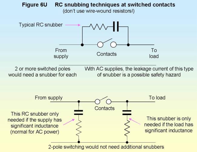
Snubbers can also use non-linear devices such as diodes, rectifiers, zeners, and a variety of surge protection devices (see Part 3 of this series) to provide an alternative path for the flyback currents, either on their own or in conjunction with RC snubbers. The higher the turn-on voltage of the device, the faster the stored energy will collapse and the quicker can be the rate of cycling of the load. Unfortunately, the higher the turn-on voltage, the greater will be the spark at the contacts, so this can lead to a compromise between rate of operation and emissions. DC circuits can use unidirectional semiconductor snubbers, remembering that the flyback voltage has the opposite polarity to the applied voltage.
A side-benefit of all spark suppression techniques is that they generally increase contact life.
6.5.2 Suppressing arcs and sparks in DC motors
In general, DC motors are a very serious source of conducted and radiated emissions, and are very difficult to suppress. The filters and other suppression devices required for them to meet emissions standards can cost more than (and sometimes bulk as large as) the motor or bell itself.
Some ‘pancake’ DC motors don’t spark because their brushes connect to a number of rotor windings at once, so there is always one of them in circuit to provide a path for the flyback currents in the windings.
Larger, more industrial DC motors with fully-enclosed metal bodies tend to emit less and be easier to suppress than lower-cost motors. Larger DC motors connected by many metres of cable to their controls or drives are able to reduce their emissions by using good quality screened cable, as long as its screen is 360o bonded at the motor’s metal terminal box (and probably to the earthed cabinet enclosure at the controlling end).
Where this technique is not sufficient, or impossible to apply (as in many motorised toys or domestic equipment such as CD players), it is best to use a motor with transient suppression fitted to its rotor. The rotor is where the energy is stored in a brushed DC motor, and is best dealt with before it causes sparks in the commutator. A ‘varistor disc’ can easily be fitted to most low-voltage DC motors, essentially connecting a varistor (voltage-dependant resistor, described in Part 3 of this series) between each pair of contacts on the commutator. For a 24V motor the varistor disc may be designed to conduct at 30V or so, and only conducts current when flyback occurs. During flyback, it conducts the energy into the neighbouring winding and limits the resulting overvoltage at the commutator to under 45V or so. This still causes sparking, but only small ones with much lower emissions.
Where a varistor-disc motor cannot be obtained, it is usually necessary to shield the motor and filter after the commutator, not always very easy to do at low cost. Metal shielded motor bodies are preferred to (crudely) catch the radiated emissions from the sparks and return them back into the motor where they came from, via the filter. The filter is also needed to reduce the conducted emissions. Since DC motor emissions are still going strong at 1GHz (and also, in fact, at 10GHz), motor shielding needs to have very few very small gaps. Motors with metal end caps and metal bodies may appear well-shielded, but the bonds between the metal parts may be poor due to paint or anodising.
A filtering technique which works well is to bond one of the commutator terminals directly to the metal motor body (the shield). The other terminal is decoupled to the motor’s metal body by a capacitor with very good high-frequency characteristics, such as an 820pF multilayer ceramic with a COG or NPO dielectric and very short leads. The capacitor must be rated to cope with the transient voltages caused by commutation. Where it is not possible to bond one of the brushes directly to the metalwork, it should be decoupled in the same way as the other brush. A low self-inductance is very important for these bonds and decoupling, and even 5mm of length or distance can be crucial. Feedthrough capacitors of around 1nF, screwed into the body of a fully metal enclosed motor and used as the brush terminals to the motor cable, often work very well indeed, although they are not inexpensive.
Correct application of shielding, bonding, and decoupling, may make the motor’s emissions low enough. If not, the next step is to add chokes to the brush leads, as close as possible to the decoupling capacitors but immediately outside the motor body. Differential chokes and across-the-line capacitors may be needed to reduce low-frequency emissions, whereas common-mode chokes and line-to-chassis capacitors are usually best at suppressing high-frequency emissions. A multi-stage filter using both types of choke may be needed in difficult cases, and is often best implemented with a PCB mounted directly on the motor end-cap at the commutator end, to keep all lead lengths low and to permit low-inductance bonding of capacitors to the motor body.
A varistor-disc motor with only very tiny sparks on its commutator should last longer before it commutator wears out, whereas a shielded and filtered motor will not benefit in this way because its sparks have not been made any smaller.
6.5.3 Suppressing arcs and sparks in electric bells
Like commutator motors, electric bells create emissions from DC to daylight. The best technique is to remove their spark gap and use an oscillator (astable) circuit to pulse current through the hammer solenoid at the hammer’s natural frequency. This is usually very much cheaper than any filtering methods. Such an electric bell could be much more reliable, and of course would require no adjustment to its spark-gap during manufacture. It may be that this is the first significant improvement in the design of electric bells since the 1880s.
6.6 Power factor correction
EN 61000-3-2 came into force on 1/1/2001 under the EMC Directive for all equipment consuming up to 16Amps/phase and connected to public low-voltage mains supplies. It limits the harmonic (non-sine wave) currents drawn by products, for all lighting equipment consuming above 25W and all other products consuming above 75W. Professional equipment rated at over 1kW has no limits to meet at the time of writing.
The problem for typical rectifier-capacitor AC-DC power converters is that they appear to the power distribution as non-linear loads because they only top up their DC storage capacitors at the peaks of the AC supply waveform. Their supply currents are discontinuous, non-sine wave, and rich in harmonics (as shown by Figure 6V).

The special problem for single-phase power supplies is that they emit triple (or triplen) harmonics (3rd, 9th, 15th, etc.), which are a particular nuisance since they add linearly in neutral conductors (no cancellation) and are a major cause of cable and transformer overheating.
In a larger installation with a lot of single-phase electronic loads (typical of a modern office) the neutral currents can reach over 1.7 times the size of the phase currents. Since many older buildings are wired with half-size neutrals, and since building neutrals aren’t fused, the fire hazard is clear.
Harmonic emissions create a number of problems for power generation and distribution, not least of which is overheating and fire (something that fire insurers are becoming increasingly aware of). There are a number of ways of dealing with this problem at the equipment and installation levels. Electronic solutions at the equipment level are the main concern here.
There are many other non-linear loads which also cause harmonic currents in the supply, such as transformers and motors; arc furnaces and welding equipment. Fluorescent lamps with magnetic ballasts have harmonic emissions too, and although they include even-order harmonics they usually don’t extend to very high frequencies. High-frequency ballasts for fluorescent lamps (including the popular ‘low energy’ filament bulb replacement products) are simply single-phase AC-DC switch-mode power supplies – with all their harmonic problems. Three-phase power converters (sometimes called 6-pulse converters) are also a source of harmonic emissions, but if operated with balanced loads they produce low triplen levels.
When an item of equipment draws (‘emits’ in EMC terminology) harmonic currents from a sine-wave AC supply, the harmonic currents are reactive and increase the VA consumption of the equipment without affecting its consumption when measured in Watts. The ratio of Watts to VA consumed by a load is known as its Power Factor (PF), so where an equipment has significant emissions of harmonics it also has a poor power factor.
A PF of 1 means that the Watts consumed equals the VA of the equipment, in which case it looks like a pure resistive load and has no harmonic emissions. AC-DC power converters with no harmonic reduction techniques tend to have PFs of around 0.6. Techniques which reduce the emissions of harmonic currents into the AC supply also improve the equipment’s PF, so they are usually called Power Factor Correction (PFC) techniques.
Don’t confuse real Power Factor (= W / VA) with the power factor traditionally used by electrical generation and distribution engineers, which is the cosine of the angle between the sine-wave supply voltage and the load current and can be adjusted by either adding capacitance or inductance to a power line. The electrical engineers’ traditional PF is based on sine wave voltages and linear loads (resistive, inductive, or capacitive) and so is actually a special case of real PF. Few, if any, power distributions these days have linear loads, and you cannot correct the PF of an electronic AC-DC power supply using the traditional methods for linear loads.
There are a number of techniques for reducing harmonic emissions (improving PF) for items of electronic equipment:
· Filtering
· Passive PFC using an inductor between bridge rectifier and DC storage capacitor
· Passive PFC using a charge pump with a suitable SMPS controller
· Active PFC using a boost regulator after the bridge rectifier
· Increasing 3f rectifiers to 6f
Filtering means simply connecting filters at the AC input to the power converter to limit the emissions of some or all of the harmonics. Because the frequencies are so low, and the currents involved are often measured in Amps, these filters can be physically large, heavy, and expensive.
Small linear power supplies have relatively high impedances in their mains transformers, which spreads their pulses of supply current in time and so reduces their harmonic content. They sometimes meet the harmonic limits without modification. As power transformers get bigger their impedance drops and the resulting current pulses into their bridge rectifiers are sharper and contain more troublesome harmonics. Larger linear supplies therefore emit harmonic currents as readily as do switch-mode power supplies, which no transformer between their bridge rectifier and their unregulated DC storage capacitor.
One solution is to add a series inductance either before or after the bridge rectifier, as in Figure 6W. This widens the conduction angle of the rectifiers and so reduces their harmonic emissions. The lowest harmonics are realised when the choke has a very large inductance, but these can be comparable in size with a mains transformer rated for the product’s full power.

It appears that single-phase rectifiers with constant-inductance choke input filters can be designed to meet the toughest harmonic limits in EN 61000-3-2 for power ratings <1500W. Choke values of 7mH to 70mH are approximately required for direct-on-line voltage-doubler rectifiers, the higher values applying at lower powers and currents. Transformers with the requisite inductance could be made, to save adding a separate component for applications where low-voltage high-current supplies are required and switch-mode techniques are not favoured.
The inductor in series with the unregulated DC capacitor resists rapid changes in current, so makes the rectifiers conduct for longer – reducing harmonic currents. The inductor must be sized so its flux does not become discontinuous at any point during a cycle. As the inductor is used on DC, care must be taken to ensure it does not saturate. The large air-gaps used to prevent saturation will emit quite strong ‘hum’ magnetic fields locally and if the inductor is not shielded these may affect the placement of other devices and the routing of cables and PCB traces nearby. It may be possible to adapt this circuit to put the inductor on the AC side, so that it sees an AC current and saturation is less of a problem.
With the right kind of switch-mode power supply (SMPS) controller it is possible to use passive ‘charge pump’ circuitry to correct power factor and reduce harmonics, as shown in Figure 6X.

An example is the Infineon TDA 1684X family (e.g. TDA 16846, TDA16847).Their load dependent frequency response for free running SMPS’s allows them to control sinusoidal switched mode power supplies featuring a PFC charge pump circuit (as well as provide a low power standby operation). For more on this technique refer (for example) to the Infineon Application Note: AN- TDA 1684X (version 1.2, dated June 2000).
Traditional SMPS converters do not have the charge-pump circuitry shown in the dotted box of Figure 6W. With the charge-pump circuitry, the current (IL) in the charge pump choke (L) becomes higher with a longer switch-on time of the switching device (T). The controller operates so as to make T’s switch-on time increase with a decreasing mains voltage, thereby increasing the current through the PFC charge pump circuit. With suitably dimensioned components this makes the load on the AC mains appear resistive. The additional stored energy in capacitor Cp makes the SMPS capable of stabilising the ripple voltage during mains zero crossings.
Adding the charge-pump circuitry does not worsen any other EMC emissions (unlike the ‘Active PFC’ technique described later). But it does increase the dissipation in T by a significant amount and so can worsen efficiency and make larger devices and/or heatsinks necessary. The waveforms of Figure 6Y show the various currents and voltages in the charge pump and SMPS circuit for an example cycle, to help understand the operation of the circuit.

Different waveforms obtain under different conditions of supply voltage and load current, although they still retain the same principle (for more on this refer to the Infineon Application Note: AN- TDA 1684X (version 1.2, dated June 2000).
The charge pump’s capacitor current peaks when the voltage across T is high. This considerably increases the dissipation in the switching transistor T, when compared with the same converter without the charge pump, requiring larger devices and/or larger heat sinks for reliable operation. However, it is possible to feed the charge pump’s capacitor from a separate winding on the transformer instead of from the switched primary winding. This can be designed in such a way as to reduce the dissipation in T to close to what it would be without a charge pump – saving cost and PCB area.
The ‘Active PFC’ technique interposes a switch-mode boost converter between the bridge rectifier and the storage capacitor, as shown in Figure 6Z. It boosts the full-wave rectified supply when it is lower than the voltage on the storage capacitor.

The rectified mains voltage is boosted under the control of an IC that causes the current into the storage capacitor to approximate a full-wave rectified sine wave. Thus the storage capacitor plus active PFC circuit looks like a resistive load to the bridge rectifier, so the whole lot appears to the AC supply like a resistor (although with little notches around zero-crossings due to the rectifiers). The boost circuit typically operates at a high frequency, even several MHz, so a filter capacitor (usually around 1mF) is required to convert the fast-switching current pulses into a reasonably-looking rectified sine wave.
Active PFC circuits have a time constant of around 0.5 seconds to smooth out load current fluctuations so that their AC supply’s simulated resistance appears to change in value slowly, not to cause harmonic emissions. This needs to be taken into account when designing the size of the DC storage capacitor. The PFC boost circuit used generates high-frequency conducted and radiated emissions which need suppressing. Usually these boost circuits are added to existing switch-mode power supplies where some filtering and shielding will already be in place, although they are likely to need modifying.
Figure 6AA is taken from an EPCOS application note on their active PFC products. The waveforms shown for VC, IL, VE and IE correspond to the points marked on the overview circuit on Figure 6Z. Figure 6AA shows how the inductor current is pulse-width-modulated and smoothed by the input capacitor to simulate a sine-wave input current. The voltage on the DC storage capacitor will have 100Hz ripple on it (or 120Hz).

Most PFC circuits will be followed by voltage regulation, usually another switch-mode converter. Control ICs are now becoming available that will manage both functions: PFC and regulation.
Figure 6BB shows an example application circuit for an EPCOS PFC controller, complete with input filtering and surge protection.

Active PFC has many advantages apart from helping to meet harmonic emissions standards, including...
Universal input
Having active PFC boost circuitry makes it easier to design power supplies which will cope with a wide range of supply voltages, such as 85 to 264V, DC to 400Hz, allowing operation from the public low-voltage mains (and some aircraft supplies) anywhere in the world.
This reduces the need for ‘country variants’, reduces stockholding, and allows faster order fulfilment.
Full power available from wall sockets
Active PFC can draw full power from wall sockets (e.g. 3kW from a UK 230V 13A plug, 1700W from a US 110V 15A plug). Previously they were typically limited to < 50% of the possible power before the fuse in the plug or the building’s over-current protection operated.
Waveform insensitivity
Some countries, especially in the developing world, can have very badly distorted supply waveforms. ‘Traditional’ power supplies are sensitive to crest factor (the ratio of peak to RMS) so do badly on distorted supplies. Active PFC helps cope with these situations.
Universal-input PFC supplies help cope with dips, sags, brownouts, and dropouts
Mains supplies everywhere suffer from dips, sags, brownouts, and dropouts. These can cause microprocessors to reset frequently, causing annoyance to users even if they don’t cause data to be lost or control systems to go out of control. A universal-input power converter running on a nominal 230V will run perfectly well, keeping its storage capacitors fully charged, on -50% mains.
The harmonic emissions from three-phase power rectifiers (AC-DC converters) can be reduced by making them six-phase. Six-phase rectifiers are often called 12-pulse converters and use the fact that the phase outputs from star and delta wound 3f transformer secondaries are 60o apart, so use both star and delta secondaries each feeding a three-phase rectifier which feeds into the DC rail, as shown by Figure 6CC.

Like three-phase converters, six-phase converters naturally have low levels of triplen harmonics (into balanced load) but the conversion to six-phase reduces their emissions of 5th and 7th harmonics too. A series inductor can be added, in the AC or DC sides, to reduce the harmonics even more (these are often called ‘line reactors’ or ‘DC link reactors’) and operate in the same way as the series inductors described earlier, but as they do not have to deal with very high levels of current ripple their design constraints are eased.
Three-phase ‘boost’ rectifiers use PWM control of power transistors (usually IGBTs) instead of ordinary rectifiers, using ‘rectifier’ circuits similar to that of Figure 6DD. When the switching rate of the PWM is much faster than 50Hz the switching functions can be replaced by their average values in the switching period.
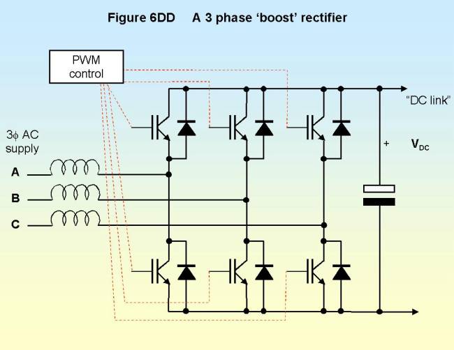
By appropriate control of the PWM switching patterns these boost rectifiers can achieve a near sine-wave input current from the mains supply, hence PFC. They can also achieve bi-directional power transfer. They have a tendency to become unstable which is usually overcome by using a large value for the DC capacitor.
7. System level techniques
There are mains harmonic reduction techniques which can be used at the level of the system or installation, but of course they don’t help equipment meet EN 61000-3-2.
Some harmonic problems in systems and installations are simply dealt with by up-rating conductors (neutrals may need double the cross-sectional area of the phase conductors) and transformers.
Star-delta transformers help remove the triplen harmonics typical of single-phase mains distributions. Their loads must be well balanced and they must be rated for the appropriate levels of zero-phase magnetic flux in their delta windings
Filters (series and parallel types) can restrict the flow of harmonic currents in areas of the mains distribution. Filters are ‘tuned’ to each problem frequency, and can interact unpredictably with existing network resonances. Filters should be left to power system harmonics experts.
‘Active filters’ are now available which are much easier to use than passive filters. A better name for these types of equipment is ‘active harmonic conditioners’ as they are not really filters but ‘anti-harmonic generators’ that take energy from the mains supply and add it back in as necessary to preserve its sine waveform. They only use the energy associated with their internal inefficiencies, since on over periods of one second or more the power they need to extract to preserve the waveshape is exactly equal to the power they need to inject.
Uninterruptible power supplies (UPSs) can be used providing they themselves have sufficiently low levels of harmonic emissions into their mains supply (check manufacturers’ data carefully).
Motor-generator sets are a traditional way of confining harmonic currents to mains conductors which are isolated form the public supply.
· Operating equipment from its own low-voltage distribution transformer is another traditional technique. The low impedance at the common point of connection to the high voltage supply reduces the effect of the harmonic currents on the public low-voltage network.
8. Conclusion to the Series
A textbook could be written about any one of the topics covered above, and I am keenly aware of the topics I have left out or dealt with in a rather brief manner. I am sure many specialists are wincing at the treatment I have given to their subjects. Many people have written to me with useful comments and suggestions, for which I am most grateful. I especially acknowledge the huge contribution made by Tomonori Sato since I wrote the first versions in 1999.
The aim of this series was to introduce the EMC non-specialist to the various issues and point to the most important and commonly-used best-practice design techniques, and I hope I have achieved this.
Theoretical background has been minimal, where it existed at all, despite the fact that an understanding of the theory behind EMC helps designers to deal with the unexpected (of which EMC often appears to have more than its fair share). The books recommended in Part 5 will be found useful in obtaining this knowledge. Many more EMC textbooks and guides exist for the interested reader.
Many of the techniques described in this series are also important for improving signal integrity. They are thus powerful competitive weapons in reducing the number of iterations during development, reducing manufacturing costs, and improving reliability in the field and enjoying lower levels of product returns and claims under warranty. They may also be helpful in reducing a company’s risk under product liability legislation. Even if the EMC Directive did not exist in the EU, or the FCC in the USA, the techniques described in these six articles would still be worth using for the real engineering and financial benefits they bring.
Eur Ing Keith
Armstrong C.Eng MIEE MIEEE
Partner, Cherry Clough Consultants, www.cherryclough.com,
Associate of EMC-UK
Phone: 01457 871 605, Fax: 01457 820 145, Email: keith.armstrong@cherryclough.com