|
Effective ESD Transient Voltages Surge Suppression in New, High Speed Circuits
By Thomas G Nagy, Director of Product Development, Cooper Electronic Technologies
Electrostatic discharge (ESD) is a frequent phenomenon occurring in nature and unfortunately in the electronics equipment environment with very damaging results. It is responsible for >25% of the semiconductor chip damage during wafer fab, through various stages of circuit assembly and on the completed and in-use electronics equipment.
Typically the discharge is a result of a human body part (finger) being in close proximity to electrically charged dissimilar materials and then subsequently to conductive contact points attached to electronic devices. The result is at best, damaged IC’s and warranty claims against the manufacturer of the end user devices
Fig. 1 Typical device damage by localized melting of metallization from ESD overvoltage surge –probably still operates, but close to total failure.
This is a serious problem so much so that the European Community, for example, has defined specific standards for the ESD suppression requirements to be met by any product sold in that economic zone. The designer therefore is obligated to provide effective ESD protection for the ever more sensitive semiconductors.
Unfortunately, this task often follows an afterthought design principle - first build the circuit without additional overvoltage transient suppression, relying on the IC on-board protection. If tests indicate sensitivity during the prototype phase then add the protection devices. Unfortunately, with the lower operating voltages, increasing frequencies and lower noise requirements, the entire design needs to be optimized and integrated and adding the protection at the end can be more expensive or impractical due to time constraints.
Generally, the ESD events are described by three primary ESD algorithms based on the type of charge process and severity of transient surge; the human body model(HBM), the charged device model(CDM) and the machine model(MM). These models define the types of transient threat, allow defining specific semiconductor chip overvoltage transient level sensitivities, and chip and assembled product test procedures. Circuit designers can test the ESD protection effectiveness of the chip and product uniformly and make quantitative comparisons between alternative solutions.
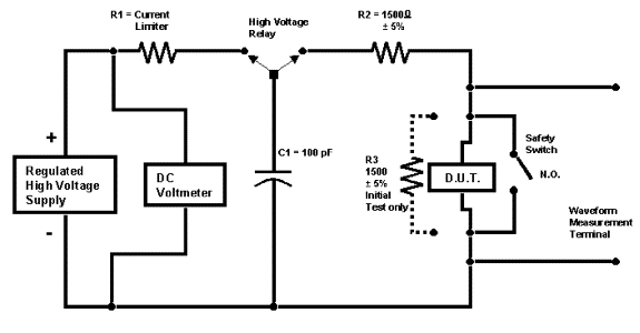
The direct transfer of charge through a series resistor such as a human finger is the most common source of ESD damage. Thus the pre-eminent ESD model is the HBM. This is represented by the discharge of a 100pF capacitor through a 1500 ohm resistor into the device under test. The commercial version of this standard has been the Mil Spec 883 Method 3015 as shown by Fig.2 below.
Fig. 2 Mil Spec 883 Method 3015 ESD HBM standard test diagram
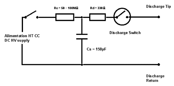
The most prevalent HBM variant is the International Electrotechnical Commission(IEC) 1000-4-2 standard that is defined by a 150pF discharge through a 330 ohm resistance. This is the recognized international test required by the EU for any product sold in that region, for example.
Fig. 3 IEC 1000-4-2 model test circuit
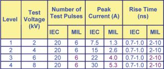
There are significant transient voltage threat and energy level differences between the two models. Designers tailor the test process to that expected for their specific application. IEC 1000-4-2 has a much faster voltage pulse rise time, more pulses applied, and higher peak current.
Fig. 4 Mil Spec vs. IEC test standards for HBM ESD event
In recent times, designers of circuits have been using a group of devices (TVS) among others, solid state devices (diodes), metal oxide varistors (MOV), thyristors, other voltage variable materials (new polymer devices), gas tubes, and simply spark gaps. These devices are positioned between the incoming surge and ground and rapidly change their resistance to a low state when the incoming voltage surge reaches a level that causes them to “turn-on” or conduct. The incoming threat is ideally partially reflected back, and the balance is partially shunted to ground through the conducting TVS device, with a smaller portion reaching the sensitive IC in the circuit.
The choice of ESD suppression devices have all had advantages and disadvantages for the designers. With the advent of the new high speed circuits some of the disadvantages have magnified.
The TVS must have very fast response to the incoming surge-the threat voltage reaches its 8+kV peak in 0.7 ns. The trigger or clamping voltage of the TVS device (in parallel with the input line) needs to be low enough to be an effective voltage divider. Some of the devices protect the circuit but wear out after just a few pulses, and/or fail in a low resistance (shorted) condition leaving the circuit with a high current drain to ground. This is, of course, deadly for the battery operated devices. Each device has its own anomolies: gas tubes carry high currents but are very slow to respond, wear out and do not recover. MOV’s have a relatively slow turn on response for high speed circuits. The silicon diodes have a very fast trigger response and low turn on voltage characteristics, but like the MOV’s and the other devices, their capacitance is relatively high. High capacitance degrades high speed signal. The higher the frequency the worst the effect of the capacitance. The new voltage variable ESD devices are the only ones currently capable of offering extremely low capacitance, very low off state current leakage, self restoring after many pulses. Then, there is the cost factor - designers want to keep the cost of passive devices to a minimum. Diodes have had very low purchase prices due to high supply volume - some of the new high frequency polymer devices are now also very competitive.
Several major design factors made the ESD suppression issue simpler in the past; higher device operating voltage/slower more robust IC devices (less sensitivity to surge), much lower operating frequencies (protection speed not as important), higher circuit impedance from lines and leaded components, and much more metal in the packaging, fewer external contacts
The electronics industry, however, has changed - explosive growth in the consumer telecommunication industry. This means more handheld (human contact) devices. Plastic has become the packaging material of choice - this means charge build up potential, in tandem with a huge number of exposed metal contacts for data transfer, charging, audio/video/RF communication functions built into the devices.
The device operating frequencies leaped from the few Khz to the Ghz ranges, causing design problems with distortion from high capacitance passive components used for ESD protection. The chip operating voltages are dropping along with much increased sensitivity for any high energy transient (localized junction heating/melting). New, high frequency digital consumer devices require very low off-state current leakage for low noise. And, in the low cost production environment, the cost cutting is the primary goal for all circuit components.
Effective ESD suppression products should, therefore, offer the designer several major benefits and features. This is not totally in order of importance but… lMust be very cost effective - all designers are under severe competitive cost constraints. l Ability to protect new consumer electronics device audio/video I/O lines, and RF connectivity ports without compromising the performance. l Ability to protect the new communication connectivity technology hardware from ESD damage. l Constant characteristics over a wide range of operating frequencies. l Sub pF capacitance in wider bandwidth circuits at multi -gigahertz frequency operation. l Minimal current leakage to ground during off state condition to keep noise minimal. l Low operating circuit signal distortion/attenuation due to the ESD suppression component. l Triggering and clamping characteristics to match circuit components’ requirements for effective protection. l Required circuit mounting characteristics, form factor and footprint. Easy installation on high speed auto insertion lines. l Maximum interchangeability between the various device alternatives preferably without circuit layout changes. l High reliability over the life of the product.
The designers’ dilemma, of course, is that the new high speed data lines need the protection even at the multi gigahertz frequencies. In addition, there are the new transmission protocols driven by the new high speed chips.
The placement of the surge suppression devices is a critically important issue. This is generic no matter what the choice of TVS device. The length of trace lead prior to the placement of the TVS should be minimum, since the fast ESD pulse can inductively induce additional voltage that works against the protective capacity of the TVS device. In addition, the fast 0.7 ns ESD pulse can induce voltages into the adjacent (parallel) leads on the circuit board. If that happens the assumption that the circuit is protected may not be true since the induced voltage paths will result in alternate paths for the surge to reach the IC. Thus, protected input lines should not be arranged next to other separate unprotected traces to avoid the issue of induced voltage in them.
The recommended PCB mounting scheme for the ESD suppression devices is that it should be:- l prior to the IC to be protected but as close to the PCB side of the attachment point of the connector/contact as possible. This eliminates the above issues. l before any resistor in series with the signal line. l Before any filtering or conditioning device including fuses. l At any other location before the IC where possibility of ESD incursion exists.
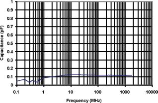
As a result of the heightened interest by the industry in methods to deal with the ESD suppression in high frequency circuits, studies have been conducted for some of the large players in the consumer electronics business. Comparative data suggests that while the trigger/clamping voltage of the low cost silicone diodes and even varistors, is very low, their high frequency circuit behaviour such as capacitance and current leakage, are not adequate for a growing number of applications. Variable voltage polymer devices, such as those from Cooper Electronic Technologies have tested at the 0.10-0.12 pF values up to 1.8 Ghz frequency range. Typical diode values are at >3pF and rising over this range.
Fig.5. The Capacitance of polymer ESD suppressors from Cooper Electronics Technologies, 0.1MHz to 1.8GHz
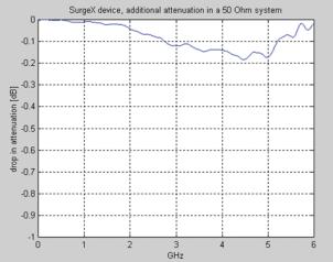
Another important characteristic required is minimal ESD suppressor influence on the circuit signal characteristics. Measurements conducted on the polymeric ESD suppressor indicated a less than 0.2 db attenuation effect up to 6 Ghz making it virtually invisible to the circuit.
Fig. 6 Additional Attenuation in a 50Ohm System due to the Cooper Electronic Technologies polymeric Esd suppressor.
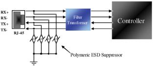
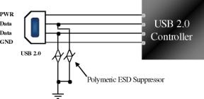
Commercial products require ESD surge protection of all the interface hardware schemes. Some of the new computers and higher end consumer electronics, for example may have most or all of the interconnect devices such as the Ethernet, USB/USB2, IEEE 1394/1394b, Audio/Video/RF ports, in addition to the traditional RS-232, RJ 11, etc ports. The traditional protection devices all have been used with varying success, however the frequency increase now indicates a need for the ultra low capacitance devices, such as the Polymeric suppressors.
Fig. 7 ESD Protection of 10Base-T/100Base-TX Ethernet (RJ-45) with polymeric ESD suppression device from Cooper Electronic Technologies.
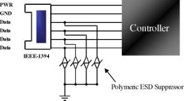
The fast data transfer protocol of the IEEE 1394/1394b (Firewire) is utilized on many new consumer electronics devices. The high data rate requires low capacitance ESD suppressors such as the polymeric Cooper Electronic Technologies Surg® devices.
Fig. 8 The IEEE-1394 (Firewire) series now speed data transfer rates up to 1,600Mbp (1394b.) The requirement is to do it without distorting the high speed connection. The diodes have too much capacitance to protect the lines without altering the signal.
Test data shows that the polymeric ESD suppressor devices can provide the ESD protection of the Firewire port with much less signal distortion than the silicone diode devices.
Fig. 9 Signal distortion comparison in circuits using Zener diodes and Polymeric ESD suppressors.
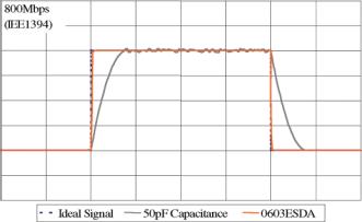
The new USB 2.0 protocol has a fast data transfer rate of 400Mbps. A device equipped with USB 2.0 will give the best performance when protected with the ultra low capacitance polymeric device with SurgX® technology from Cooper Electronic Technologies. This will result in much less data distortion than if zener diodes or multi layer varistors are used for ESD protection
Fig. 10. ESD protection of USB 2.0 devices with polymeric ESD suppression device.
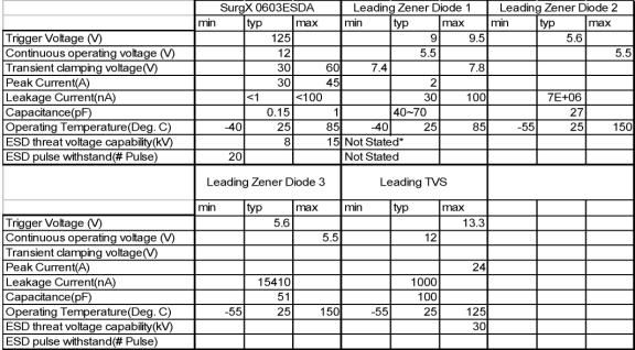
To be noted that the designers of the various devices used for ESD/ suppression are constantly developing new variations of the suppressors with improved characteristics, and are pushing the envelope of all traits. Some of the comparative characteristics are noted in Fig. 11 below.
*The values are obtained from actual testing under IEC 61000-4-2 specification. At this point the designer will see from the available information that:- l Polymeric ESD suppressors such as the SurgX® devices from Cooper Electronic Technologies, give the lowest capacitance (<.1 pF) and leakage current values (<1nA), coupled with a sub nS turn-on spec. and the ability to recover even from over stressed condition. l Silicone diodes currently have the lowest clamping voltages but much higher capacitance values, and no ability to recover it overstressed. Thomas Nagy is the Director of Product Development for the Overvoltage Protection Product Group at Cooper Electronic Technologies, the electronics business unit of Cooper Bussmann and can be contacted on Tel: +1 561 752 5019. http://www.cooperet.com/
|